- ISO 9001:2015 Certified
- Fast Turnaround
- Worldwide Shipping
PCB Test services by FX PCB ensure every circuit board meets strict quality standards. We provide AOI inspection, flying probe testing, X-ray inspection, electrical testing, and reliable PCB manufacturing.
PCB Test is an essential part of our manufacturing process at FX PCB. Every printed circuit board undergoes advanced inspection and testing procedures to ensure reliability, precision, and compliance with international quality standards before shipment.
1 Inspect the Overall Appearance:
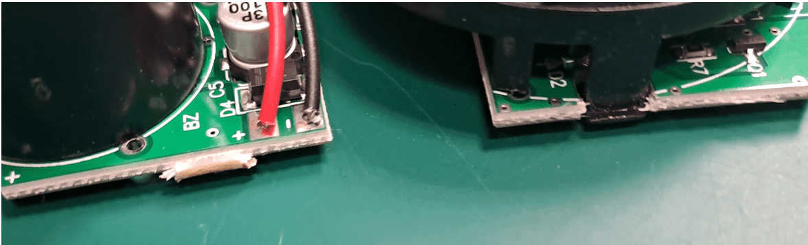
Begin by looking at the PCB as a whole. Check for any obvious physical damage, such as cracks, delamination, or warping.
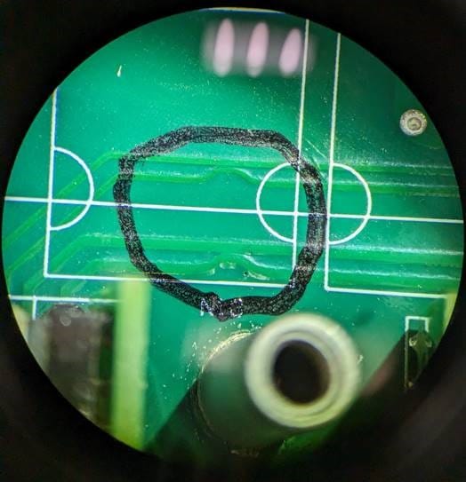
2 Check for Solder Mask Defects:
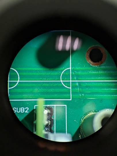
Ensure that the solder mask is the right color that customer need and it covers all areas it’s intended to. Look for:
3 Check for Silkscreen missing or correctly placed.
A, silkscreen color is correct
B, Ensure that the UL or datedcode added per customer’s request
C, Missing of incomplete silkscreen
D, overlapping or silkscreen on pad
E, silkscreen are clear, legible and correctly placed
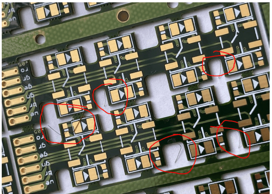
4 Look for Foreign Objects:
5,Inspect for Conformal Coating, Peekable mask or Kapton (if applicable):
6 Verify cleanliness:
7 Document Findings:
Tips:
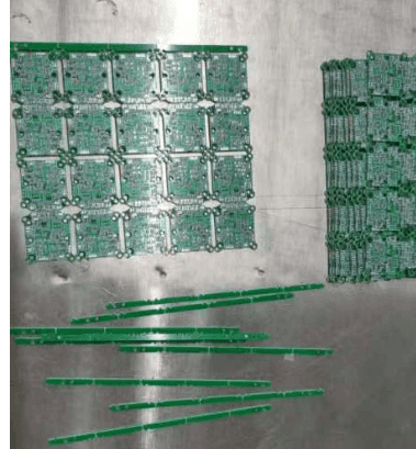
1,Firstly the worker will check the panelized way is right per customer’s drawing( right quantity in one panel), and the edge added correctly with fiducial holes or marks.
2, we will use the calipers and two-dimensional measuring instruments to measure the size. these two ways are different in their methodology, precision, and suitability for specific applications.
Here are the key differences between the two:
Measuring the V-cut depth of a PCB (Printed Circuit Board) involves determining the depth of the V-groove or score line that separates individual PCBs on a panel. This measurement is crucial for ensuring that the boards can be cleanly separated without causing damage or if it is so easy to be broke during assembly.
Tips:
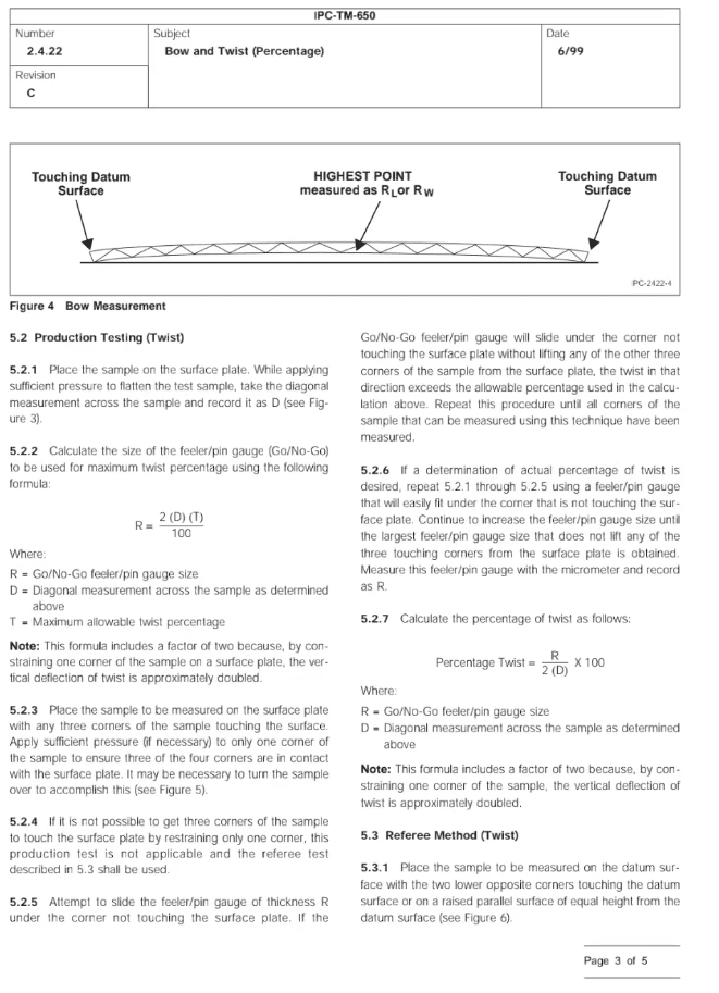
Warp and Twist measurement
Measuring warp and twist on a Printed Circuit Board (PCB) involves evaluating the flatness and planarity of the board’s surface. This is important for ensuring that the PCB will fit properly into an enclosure or assembly without causing mechanical stress or electrical issues.
Materials and Tools Needed:
Tips:
Remember that using an XRF spectrometer requires proper training and adherence to safety guidelines. If you are unfamiliar with the specific instrument, consult the user manual or seek guidance from a qualified expert.
Regularly checking and verifying warp and twist is an important part of quality control in PCB manufacturing, especially for applications where flatness is critical.
Conducting open and short tests on a Printed Circuit Board (PCB) is crucial for several reasons:
2. Quality Assurance:By performing open and short tests, manufacturers can verify that the PCB meets the specified electrical requirements. This ensures that only functional and reliable boards are shipped to customers.
3. Preventing Field Failures:Detecting and rectifying open and short circuits during manufacturing prevents faulty PCBs from reaching end-users. This helps reduce the likelihood of field failures and costly product recalls.
4. Component Verification:Open and short tests verify that all components are correctly placed, soldered, and connected on the PCB. This includes checking for correct polarity, orientation, and proper soldering.
5. Reliability and Longevity Assurance:Ensuring that there are no open or short circuits on the PCB contributes to the long-term reliability and functionality of the electronic device or system in which it is used.
6. Preventing Component Damage:Detecting short circuits helps prevent components from being exposed to excessive current, which could potentially damage or destroy them.
7. Compliance with Design Specifications:Open and short tests confirm that the PCB meets the design specifications and requirements outlined in the design documents.
8. Compatibility and Interoperability:Open and short tests ensure that the PCB will work correctly with other components and systems within the final product, preventing compatibility issues.
9. Reducing Rework and Scrap:Identifying and rectifying open and short circuits early in the manufacturing process minimizes the need for costly rework or scrap, ultimately improving production efficiency and reducing costs.
10. Compliance with Industry Standards:Many industries have specific quality and performance standards that PCBs must meet. Open and short testing helps ensure compliance with these standards.
Verification of Manufacturing Process: Open and short tests also serve as a means of verifying the quality and effectiveness of the PCB manufacturing process itself.
In summary, open and short testing is a critical quality control step that helps guarantee the electrical integrity and functionality of PCBs, ultimately contributing to the production of high-quality electronic devices or systems.
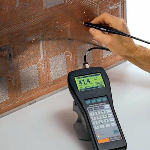
Measuring the thickness of gold and nickel plating on a Printed Circuit Board (PCB) involves using specialized equipment and techniques. Here’s a step-by-step guide for both gold and nickel thickness measurements:
Using an X-ray fluorescence (XRF) spectrometer to test the gold and nickel thickness of a Printed Circuit Board (PCB) involves the following steps:
Materials and Tools Needed:
Tips:
Remember that using an XRF spectrometer requires proper training and adherence to safety guidelines. If you are unfamiliar with the specific instrument, consult the user manual or seek guidance from a qualified expert.
Regularly checking and verifying warp and twist is an important part of quality control in PCB manufacturing, especially for applications where flatness is critical.
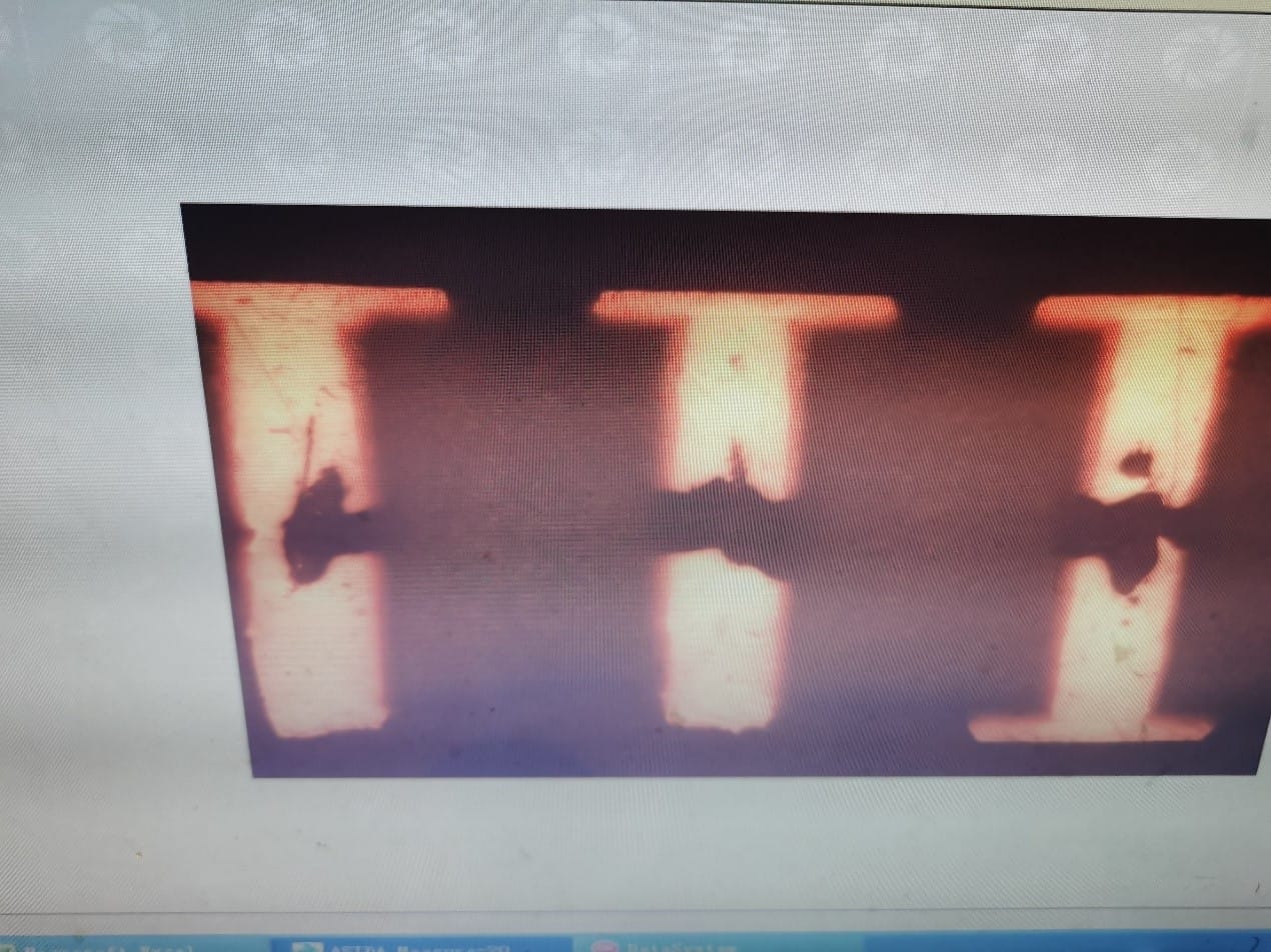
Solderability testing of a Printed Circuit Board (PCB) assesses the ability of the PCB’s surface to form a reliable and consistent solder joint. This is a crucial step in PCB manufacturing to ensure that components can be soldered effectively during assembly. Here’s a step-by-step guide for conducting a solderability test:
Materials and Tools Needed:
Important Considerations:
By following these steps, you can effectively conduct a solderability test on a PCB to ensure the quality and reliability of the solder joints during assembly.
Impedance control testing is a critical step in ensuring that a Printed Circuit Board (PCB) meets the specified impedance requirements. This is particularly important for high-speed digital and RF applications where maintaining precise signal integrity is crucial.
By performing impedance control testing, you ensure that your PCB design meets the specified requirements, ultimately leading to a reliable and high-performance electronic device.
Performing a tensile test on a Printed Circuit Board (PCB) is not a standard procedure, as PCBs are primarily designed for electrical connections rather than mechanical testing. However, in certain specialized applications or research scenarios, a tensile test might be conducted for specific purposes. Here’s a guide on how to perform a tensile test on a PCB, along with the reasons why you might consider doing so:
How to Perform a Tensile Test on a PCB:
Materials and Tools Needed:
Please note that tensile testing PCBs is not a standard practice and should be carried out by professionals with expertise in both mechanical testing and PCB technology. It is also important to remember that PCBs are primarily designed for electrical functionality, and their mechanical properties are typically not their primary consideration.
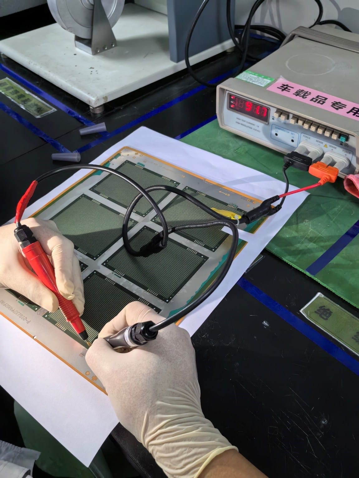
Conducting a low resistance test on a Printed Circuit Board (PCB) is crucial to ensure that there are no unintended short circuits or excessive resistances that could affect the functionality of the board. Here’s a step-by-step guide on how to perform a low resistance test on a PCB:
Materials and Tools Needed:
By following this procedure, you can effectively perform a low resistance test on a PCB to ensure its electrical integrity and functionality.
Customer can still choose other test, like salt spray test, voltage withstand test, high and low temperature cycle test and etc.

High Precision drilling for HDI boards Min Hole Size : 0.075mm
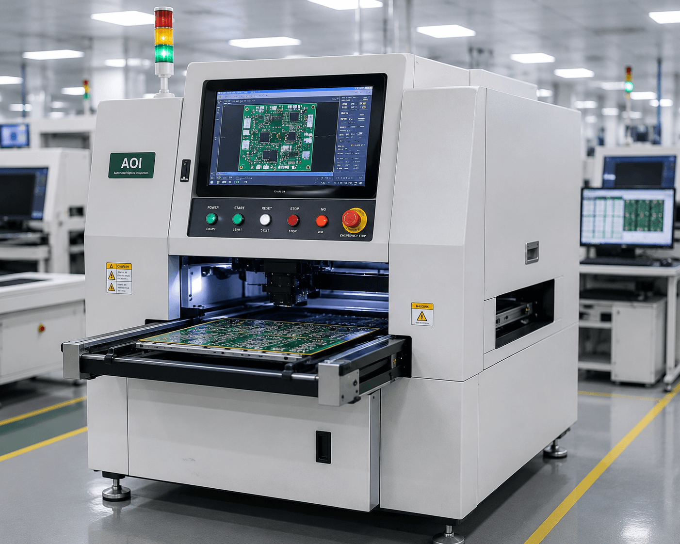
AOI Automatic optical inspection for solder and component defects.
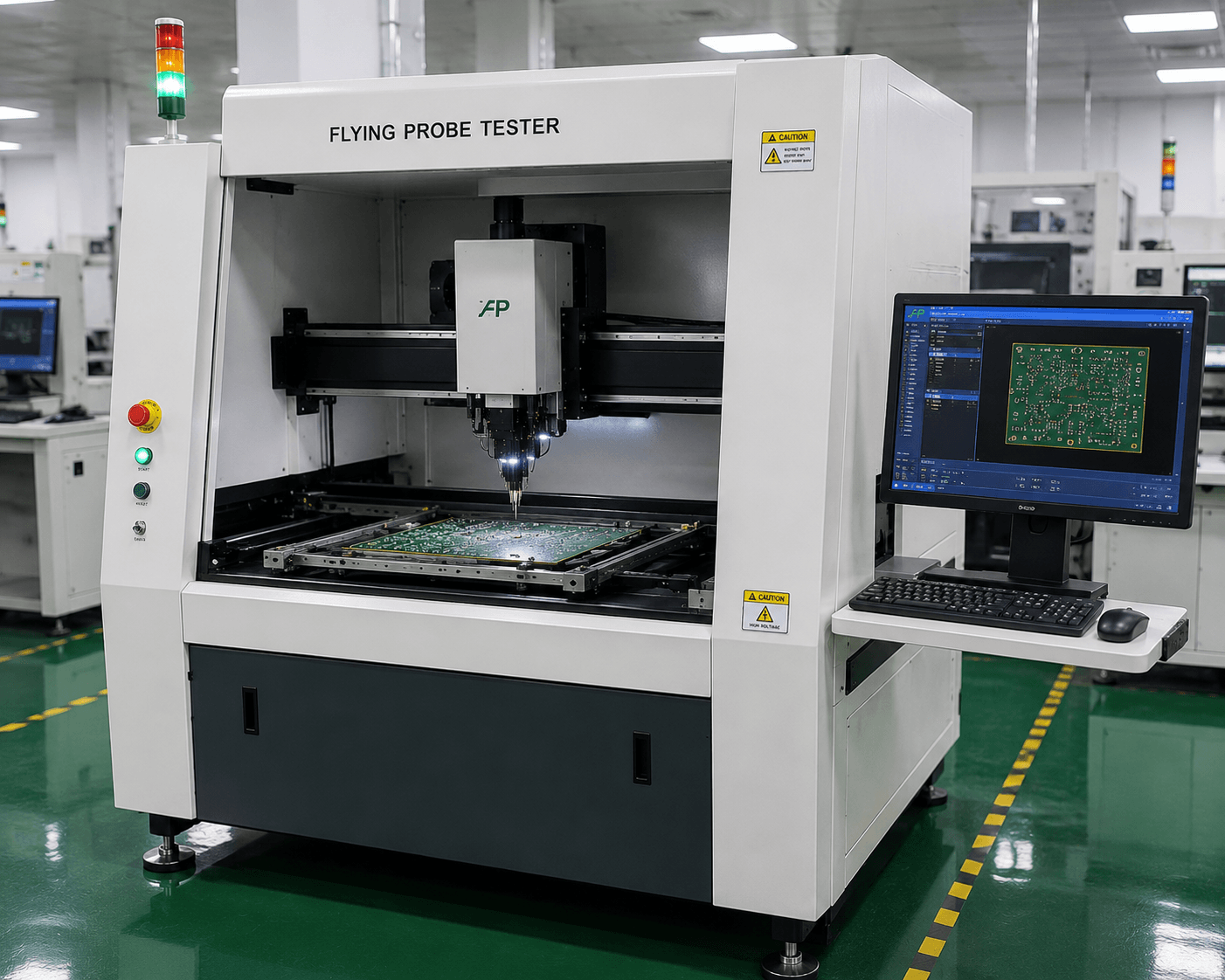
In circuit for prototypes and small batch PCB testing
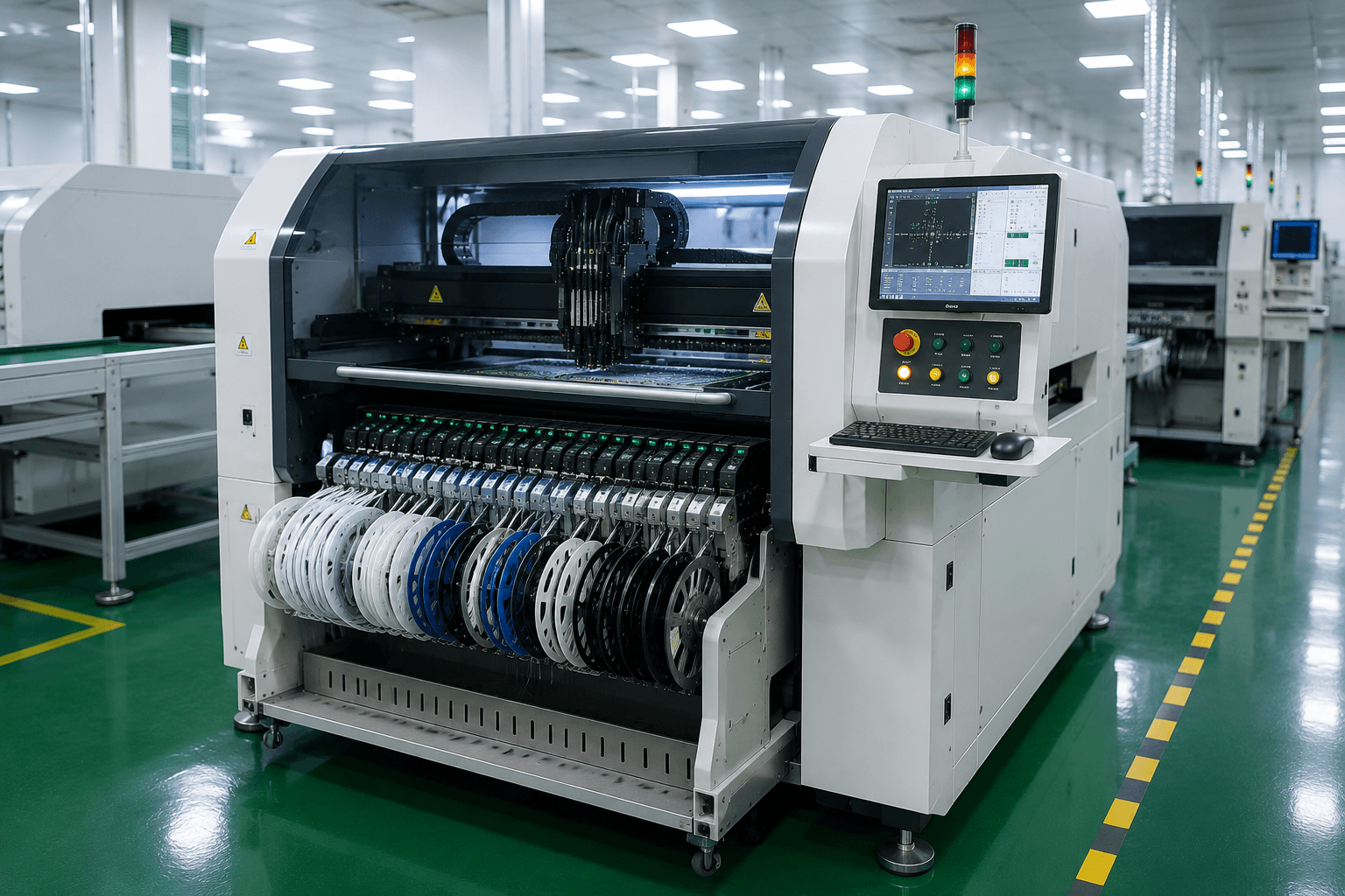
High speed placement for accurate and efficient SMT assembly
WhatsApp us