Introduction
Semiconductor fabrication is the core manufacturing process behind every modern electronic device—from smartphones to automotive control units. Yet most electronics engineers, PCB designers, and product developers have only a limited visibility into how chips are actually made.
This knowledge gap matters. The quality, yield, and performance characteristics of a fabricated semiconductor chip are determined well before it reaches a circuit board. Understanding what happens inside a fab gives engineers a meaningful advantage in component selection, design-for-manufacturability decisions, and supply chain management.
This guide covers what semiconductor fabrication is, how the process works step-by-step, what drives quality and yield, and where common misconceptions lead engineers astray.
Key Takeaways
- Semiconductor fabrication builds integrated circuits (ICs) on silicon wafers through layered photochemical and thermal steps in ultra-clean environments
- The core process repeats photolithography, doping, deposition, and etching hundreds of times to pattern transistors at nanoscale precision
- Cleanroom class, process node size, and lithography precision determine device performance and yield
- Semiconductor fabrication differs from PCB fabrication: chips are made in specialized foundries, packaged, then assembled onto circuit boards
- Understanding fabrication helps engineers make smarter decisions about component selection and manufacturing partnerships
What Is Semiconductor Fabrication?
Semiconductor fabrication is the industrial process of creating integrated circuits (ICs) on a silicon substrate by building up precisely patterned layers of conductive, insulating, and semiconducting materials at microscopic or nanoscopic scale.
The fundamental goal is to transform a bare silicon wafer into a functional chip containing billions of transistors, resistors, and capacitors interconnected by metal wiring—all within an area smaller than a fingernail. Modern high-performance chips like the AMD Instinct™ MI300X contain 153 billion transistors, manufactured on 5nm and 6nm process nodes.
Semiconductor fabrication is not the same as PCB fabrication. These three manufacturing stages are distinct:
- Semiconductor fabrication — creates the chip die at wafer level inside specialized facilities called fabs or foundries
- PCB fabrication — creates the circuit board substrate that packaged chips mount onto
- PCBA (PCB assembly) — solders those packaged chips onto the bare board using SMT or through-hole processes
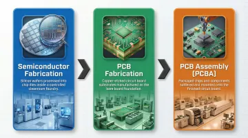
Semiconductor fabrication ends once the chip is packaged. At that point, PCB assembly takes over — which is where SFX PCB operates, building the boards and assemblies that bring finished chips into working products.
Why Semiconductor Fabrication Matters in Modern Electronics
Semiconductor fabrication is the upstream foundation for all electronics. Every microprocessor, memory chip, sensor, and power management IC used in consumer electronics, automotive systems, medical devices, industrial automation, and telecommunications begins as a fabricated wafer. The quality of that fabrication process determines everything downstream — from chip yield rates to the reliability of the end product in the field.
Modern electronics demands capabilities that make semiconductor fabrication critical:
- Process nodes measured in nanometers determine how many transistors fit on a chip — smaller nodes mean faster speeds, lower power draw, and more compact designs
- Transistor density directly drives computational power: the NVIDIA H100 GPU packs 80 billion transistors onto a 4nm process
- Reliability requirements in aerospace, medical devices, and 5G telecommunications set strict tolerances that only consistent fab quality can meet
These technical demands also shape how the industry is structured — and that structure directly affects engineers sourcing components.
The semiconductor industry operates under two primary business models. Fabless companies design ICs but outsource fabrication to foundries like TSMC or Samsung Foundry. Integrated manufacturers handle both design and fabrication in-house. For engineers, this distinction affects lead times, supply chain risk, and component availability. According to the Semiconductor Industry Association, fabless suppliers now account for a record 34.8% share of global IC sales, growing at double the rate of traditional integrated manufacturers.
How Semiconductor Fabrication Works: The Complete Process
Semiconductor fabrication is a planar process—each step is applied to the entire wafer surface simultaneously. The complete device is built layer by layer through repeated cycles of patterning, etching, doping, and deposition. A modern IC typically requires over 100 individual process steps, with photolithography repeated more than 60 times for different layers.
Step 1: Silicon Wafer Preparation
The process begins with a single-crystal silicon ingot grown from highly purified silicon using the Czochralski (CZ) method. Raw polysilicon feedstock achieves purity levels of 11N (99.999999999%), with impurity concentrations controlled to just 0.01 parts per billion.
The ingot is sliced into thin discs called wafers, polished to atomic flatness, and cleaned to remove all surface contaminants. Commercial production predominantly uses 150mm, 200mm, and 300mm diameter wafers, with 300mm being the contemporary standard for leading-edge facilities. The wafer serves as the blank physical substrate on which the entire device is constructed.
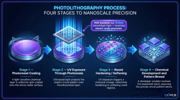
Step 2: Photolithography (Patterning)
Photolithography transfers circuit patterns onto the wafer surface using light-sensitive chemicals (photoresists) and photomasks. The process works like photography for microchips:
- A uniform photoresist layer coats the wafer
- UV or deep-UV light shines through a patterned photomask onto the resist-coated wafer
- Light selectively hardens or softens areas of the resist
- Chemical development removes exposed (or unexposed) resist, revealing target areas of underlying material
This step repeats for every new layer and is the most critical and expensive step in fabrication. ASML's standard EUV lithography tools cost around €150 million, while next-generation High-NA EUV systems are priced at €350-€400 million per system. EUV (Extreme Ultraviolet) lithography uses 13.5nm wavelength light and became standard for critical layers at the 7nm node and below.
Step 3: Doping—Ion Implantation and Diffusion
Doping intentionally introduces impurities (dopants) into silicon to make specific regions electrically conductive in controlled ways. Ion implantation is the standard industrial method—it shoots high-energy dopant ions directly into the exposed silicon surface, allowing precise control over both concentration and depth.
Common dopants include:
- N-type dopants: Phosphorus (P) and Arsenic (As)—Group V elements that provide free electrons
- P-type dopant: Boron (B)—a Group III element that creates electron vacancies (holes)
After implantation, a high-temperature annealing step (600°C to 1,100°C) repairs crystal lattice damage and electrically activates dopants by moving them into substitutional sites. Modern fabs use Rapid Thermal Anneal (RTA) or spike anneals to minimize unwanted dopant diffusion while achieving activation.
Step 4: Thin-Film Deposition (Oxidation and CVD)
With dopant regions defined and activated, the next step builds the insulating and structural layers that isolate, protect, and connect those regions. Thin films of silicon dioxide (SiO₂), silicon nitride, and polycrystalline silicon are deposited onto the wafer surface through several processes:
Thermal Oxidation (900°C to 1,200°C):
- Dry oxidation: Uses pure oxygen (O₂) to produce dense, high-quality films ideal for thin gate oxides
- Wet oxidation: Uses water vapor (steam) for faster growth of thicker oxide layers used in field isolation
Chemical Vapor Deposition (CVD):
- Exposes the wafer to volatile precursor gases that react or decompose on the substrate surface
- Low-Pressure CVD (LPCVD): Higher-temperature process for dense, stoichiometric films
- Plasma-Enhanced CVD (PECVD): Lower-temperature process (<400–450°C) essential after temperature-sensitive structures are formed
- Atomic Layer Deposition (ALD): Deposits films one atomic layer at a time for highly conformal coatings
These layers serve as insulators, gates, sidewall spacers, and structural components within the device.
Step 5: Etching and Pattern Transfer
Once a pattern is defined in photoresist and desired films are deposited, etching removes unwanted material:
Wet Etching:
- Uses liquid chemical baths to remove material
- Etches isotropically (equally in all directions)
- Undercuts the mask layer, making it unsuitable for sub-micron features
Dry Etching (Plasma or Reactive-Ion Etching, RIE):
- Uses energized gas ions to achieve highly anisotropic, vertically precise material removal
- Preferred for sub-micron features because it preserves edge sharpness critical to device geometry
- Atomic Layer Etching (ALE) removes material one atomic layer at a time for angstrom-level control
Anisotropic dry etching is indispensable for fabricating high-aspect-ratio features in modern semiconductors like FinFETs, DRAM capacitors, and 3D NAND flash.
Step 6: Metallization, Testing, and Packaging
After all active device layers are complete, the wafer moves through three distinct finishing phases:
Metallization (Back-End-Of-Line, BEOL) Metal interconnect layers are deposited, patterned, and etched to wire all transistors and components together. The industry transitioned from aluminum to copper in the late 1990s because copper offers lower electrical resistance and better electromigration resistance. Modern advanced-node chips feature 18 or more metal layers, separated by dielectric films and connected through vias.
Wafer Probe Testing (Wafer Sort) The completed wafer undergoes electrical testing to identify known-good die before the costly packaging process. Each die is probed, defective chips are screened out, and a wafer map records which die are functional.
Dicing and Packaging The wafer is cut into individual dies. Each functional die is placed into a protective housing—plastic or ceramic—with wire bonds or solder bumps forming its external electrical connections. Once packaged, the chip is ready for PCB mounting.
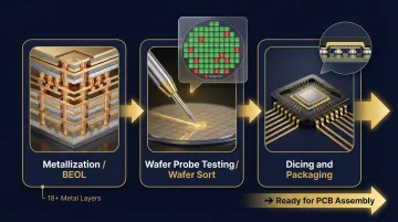
This is where semiconductor fabrication ends and PCB assembly begins. Packaged chips are soldered onto bare boards using SMT or through-hole processes—the step where a PCBA manufacturer takes over from the chip fab.
Key Factors That Affect Semiconductor Fabrication Quality
Process Node and Feature Size
The process node (e.g., 7nm, 5nm, 28nm) defines the minimum transistor gate length achievable in fabrication. Smaller nodes allow denser and faster chips but require more advanced lithography equipment.
Leading foundries offer a wide range:
- TSMC's 3nm (N3) in high-volume production, preparing for 2nm
- Mature nodes: 28nm, 65nm, 180nm still dominate many commercial applications
Most commercial applications use mature nodes (28nm and above) which offer a better balance of cost and performance. Mask sets alone for 5nm or 7nm chips cost $3–5 million, while wafer prices on mature nodes are an order of magnitude lower.
Cleanroom Class and Contamination Control
Semiconductor fabrication must be performed in ISO 14644-1:2015 classified cleanrooms (typically ISO Class 1 to Class 5) because a single particle of dust can ruin an entire chip.
Leading fabs operate with:
- ISO Class 5 in general process areas
- ISO Class 2 in localized mini-environments where wafers are processed
A single particle landing on a critical area causes a fatal defect, rendering the chip useless. The concept of critical particle size drives yield management: defect budgets set maximum allowable particle concentrations to hit target yield rates.
The yield rate (percentage of functional dies per wafer) is one of the most important economic metrics in a fab.
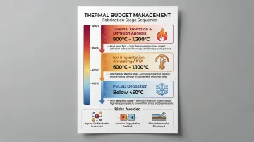
Thermal Budget and Process Sequencing
Many fabrication steps involve high temperatures (700°C–1,200°C) that cause dopants to diffuse and materials to stress. The cumulative thermal budget must be carefully managed across the entire process sequence to avoid:
- Unintended dopant redistribution
- Junction degradation
- Film delamination
Process steps are deliberately sequenced to apply high-temperature treatments before thermally sensitive layers are added. For example, thermal oxidation and diffusion anneals occur at 900°C–1,200°C, while later-stage processes use lower-temperature PECVD (<450°C) to avoid damaging existing structures.
Lithography Precision and Alignment
Each photolithography step must align perfectly with the previous layer. Misalignment on the order of nanometers can bridge circuits or open connections, causing device failure.
Modern lithography for advanced nodes requires sub-nanometer overlay accuracy. Misalignment is a primary source of defect-related yield loss. To counter this, fabs deploy Advanced Process Control (APC) strategies that:
- Collect on-product overlay data from metrology systems
- Feed measurements back into lithography scanners in real time
- Correct alignment errors before they propagate across the wafer
Materials Purity and Chemistry Consistency
The purity of silicon wafers, dopant gases, photoresists, etch gases, and CVD precursors determines electrical performance and device reliability.
Statistical Process Control (SPC) is the standard industry practice for quality management. Fabs use SPC to:
- Monitor process stability using control charts with upper and lower control limits (typically ±3 standard deviations)
- Detect variations that indicate special causes requiring corrective action
- Maintain consistent output across thousands of wafers per month
Even minor drift in a single input chemistry can cascade into measurable yield loss at scale.
Common Misconceptions About Semiconductor Fabrication
Misconception: Semiconductor Fabrication and PCB Fabrication Are the Same Process
These are entirely different manufacturing disciplines. Semiconductor fabrication creates the chip die at wafer level inside a cleanroom foundry. PCB fabrication creates the circuit board substrate. PCBA (PCB assembly) mounts packaged chips onto that board. Conflating them leads to incorrect assumptions about lead times, tolerances, and supplier capabilities.
SFX PCB, for example, offers 18+ specialized PCB fabrication technologies including rigid FR4 (1-68 layers), flexible PCBs, rigid-flex hybrids, and metal-core boards (aluminum, copper) with thermal conductivity up to 400 W/MK. These are board-level substrates onto which packaged semiconductor chips are assembled—not the chips themselves.
Misconception: All Semiconductor Fabs Are Equivalent
Fabs differ significantly by the process nodes they support, the materials and equipment available, and the product types they specialize in (logic, memory, analog, RF, power). A fab optimized for advanced 3nm logic does not produce the same product as a mature-node fab running 180nm analog processes. Selecting the wrong fab for a given process node is a common—and costly—design oversight.
Misconception: Smaller Process Nodes Always Mean Better Performance
While advanced nodes offer better transistor density and switching speed, they also introduce higher leakage currents, greater sensitivity to supply voltage variation, and significantly higher unit cost.
For industrial, medical, and automotive applications, mature nodes often win on reliability, operating temperature range, and production longevity. Two real-world examples:
- Renesas RH850/U2C automotive MCU — built on 28nm, certified to ISO 26262 ASIL D functional safety standards
- Infineon AURIX™ TC4Dx automotive MCU — also 28nm, designed for vehicle safety-critical control systems
In safety-critical designs, process node selection follows reliability and lifecycle requirements first—raw performance density is secondary.
Conclusion
Semiconductor fabrication is a complex, multi-step planar process that transforms raw silicon into the ICs that power every segment of modern electronics. Understanding it, even at a conceptual level, gives engineers and product developers a meaningful advantage in component selection, design-for-manufacturability decisions, and supply chain management.
The quality, yield, and performance of a fabricated chip are determined well before it reaches a circuit board. That makes fab knowledge relevant not just to chip designers, but to anyone building products that depend on reliable electronics — including engineers working closely with PCB and PCBA manufacturing partners.
The global semiconductor market reached $630.5 billion in 2024, with projections approaching $1 trillion by 2026. Demand is expanding across every major sector:
- Computers/AI: 34.9% of market demand
- Communications: 33%
- Automotive: 12.7%
- Industrial: 8.4%
For engineers who understand how fabrication constraints shape component performance — and how those constraints flow downstream into PCB design — that context translates directly into better product decisions.
Frequently Asked Questions
What is fabrication in electronics?
In the semiconductor context, fabrication means the wafer-level process of building integrated circuits through photolithography, doping, deposition, and etching inside a cleanroom foundry. More broadly, the term covers any manufacturing process that creates electronic components or assemblies.
What are the main steps in semiconductor fabrication?
The core stages are: silicon wafer preparation, photolithography (patterning), doping (ion implantation and diffusion), thin-film deposition (oxidation and CVD), etching, metallization, and final testing and packaging. A full modern IC process may cycle through subsets of these steps more than 100 times.
What is the difference between a semiconductor fab and a PCB manufacturer?
A semiconductor fab (foundry) manufactures integrated circuit dies at wafer level using nanoscale processes in cleanrooms. A PCB manufacturer produces the substrate board onto which packaged chips are later assembled. These are separate steps in the electronics supply chain with completely different equipment, facilities, and expertise.
What is meant by a semiconductor process node?
A process node (such as 7nm, 28nm, or 180nm) refers to the minimum feature size a fabrication process can reliably achieve, historically tied to transistor gate length. Smaller nodes pack more transistors per chip for higher performance but at greater cost; mature nodes trade raw performance for reliability and lower cost.
How long does semiconductor fabrication take?
A modern advanced-node chip typically takes 10 to 14 weeks from blank wafer to finished, tested die. Sequential process steps, cleanroom scheduling, and quality inspections all contribute to that timeline. Simpler or mature-node processes can be completed faster.
Why does semiconductor fabrication require a cleanroom?
Even a sub-micron dust particle can block photolithography patterns or create film defects, causing transistors to fail. Cleanrooms tightly control airborne particulates, temperature, humidity, and vibration to protect wafer yield and maintain consistent performance across every batch.