The FPCB market is experiencing explosive growth. According to Grand View Research, the global flexible printed circuit board market is projected to reach $50.90 billion by 2030, expanding at a 13.7% compound annual growth rate. This surge is driven by rising demand across consumer electronics (especially foldable smartphones), automotive electrification, medical wearables, and industrial automation—sectors where space, weight, and reliability are critical.
This guide covers the essential aspects of flexible PCBs: how they're constructed (layers and materials), the five main types, key advantages over rigid boards, design challenges, and real-world applications across industries. Whether you're designing a wearable health monitor or an automotive control system, understanding flexible PCB technology will help you make informed decisions about when and how to use it.
Key Takeaways
- Flexible PCBs use a bendable polymer substrate (usually polyimide) instead of rigid FR-4, enabling them to flex, fold, or conform to tight spaces
- Five main configurations exist: single-sided, double-sided, multilayer, rigid-flex, and sculptured flex circuits
- Key advantages include 60-75% weight and space savings, elimination of bulky connectors, and superior vibration resistance
- Upfront costs run 3-8x higher than rigid PCBs, but total system cost often drops once connector and assembly savings are factored in
- Common applications include consumer electronics, automotive systems, medical devices, and aerospace wherever compact or non-planar routing is required
How a Flexible PCB Is Built: Layers and Materials
Base Substrate Layer
The foundation of any flex PCB is its substrate—the flexible polymer film that gives the board its bendability. Polyimide (PI) dominates high-reliability applications due to exceptional thermal stability and chemical resistance. DuPont Kapton polyimide film can withstand temperatures from -269°C up to 400°C, making it suitable for standard reflow soldering (260°C peak) and harsh environments. Polyimide substrates typically range from 12 µm to 125 µm thick, with thinner films offering greater flexibility and thicker films providing more rigidity.
Polyester (PET) serves as a lower-cost alternative but comes with significant limitations. PET degrades above 80°C and cannot survive standard reflow soldering, restricting it to low-temperature applications using conductive adhesives. While PET costs roughly 1.5x a rigid PCB versus polyimide's 4x premium, it's limited to static sensors, membrane switches, and RFID tags where thermal exposure is minimal.
Substrate thickness directly affects stiffness: a 25 µm polyimide film bends easily around tight radii, while a 125 µm film requires larger bend radii and behaves more rigidly. Designers must balance flexibility requirements against mechanical support needs.
Bonding Adhesive Layer
Copper foil doesn't bond directly to polymer substrates—an acrylic or epoxy-based adhesive layer bridges the two. However, adhesive performance often becomes the limiting factor for thermal load tolerance. Its maximum operating temperature and bonding strength under thermal cycling determine how much heat the flex circuit can handle before delamination occurs.
For high-reliability applications, adhesiveless constructions eliminate this weak link by directly laminating copper to polyimide, improving thermal cycling performance and allowing tighter bend radii.
Conductive Copper Layer
Copper foil serves as the conductor in flex PCBs, available in two distinct forms with dramatically different fatigue characteristics:
| Copper Type | Manufacturing | Grain Structure | Flex Fatigue Life | Best Application |
|---|---|---|---|---|
| Rolled-Annealed (RA) | Mechanically rolled and heat-treated | Horizontal, layered | 1,000,000+ cycles at 5mm bend radius | Dynamic flex (hinges, wearables) |
| Electrodeposited (ED) | Electroplated onto drum | Vertical, columnar | Fails under 1,000 cycles | Static bend-to-install |
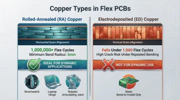
Using ED copper in dynamic flex applications guarantees premature trace fracturing along vertical grain boundaries. RA copper's ductility makes it mandatory for any application involving continuous movement: foldable phone hinges, wearable sensors, or robotic joints.
Coverlay and Surface Finish
The coverlay is a flexible polyimide film with adhesive that covers and protects copper traces, equivalent to solder mask on rigid PCBs. Openings in the coverlay expose pads for component soldering and connector attachment.
Surface finishes prevent copper oxidation and ensure solderability:
- ENIG (Electroless Nickel Immersion Gold): Premium flat surface for fine-pitch components, excellent shelf life, but susceptible to "black pad" defects from poor process control that cause brittle solder joints
- ENEPIG (adds Palladium layer): Eliminates black pad risk, preferred for aerospace and medical high-reliability applications
- OSP (Organic Solderability Preservative): Low-cost, environmentally friendly, but limited shelf life and degrades through multiple reflows
- Immersion Silver: Good electrical performance for high-frequency circuits, but sensitive to sulfur tarnishing
- Immersion Tin: Budget-friendly but carries tin whisker risk (conductive crystals causing shorts)
Stiffeners for Mechanical Support
Stiffeners—typically FR-4 or thicker polyimide—are laminated to specific regions where mechanical rigidity is needed. Common applications include areas under heavy connectors, large components, or ZIF (zero insertion force) connector interfaces. Stiffeners reduce stress on solder joints during connector insertion and prevent flexing in areas that should remain rigid.
Stiffeners are attached after fabrication using pressure-sensitive adhesive or thermal bonding. Placement is critical: positioning them too close to bend zones creates stress concentration points that accelerate failure.
Types of Flexible PCBs Explained
Single-Sided Flex Circuits
Single-sided flex circuits feature one conductor layer on a single side of the substrate: the simplest and most cost-effective flex configuration available. Components can only be accessed from one side, which limits routing complexity but maximizes flexibility.
These circuits excel in dynamic flex applications requiring high bend cycles, such as printer heads, camera modules, and simple sensor interconnects. The single copper layer minimizes total thickness, allowing tighter bend radii than any multilayer alternative.
Double-Sided Flex Circuits
Double-sided flex circuits place conductor layers on both sides of the substrate, connected by plated through-holes (vias). This configuration enables more complex routing and allows component placement on either side. The crossover connection advantage—routing traces on opposite sides that cross paths without shorting—makes double-sided flex ideal for higher-density designs.
Real-world example: Laptop touchpad-to-motherboard connections use double-sided flex circuits to route multiple signal traces through a narrow, folding flex tail while maintaining reliable electrical connections through hundreds of thousands of open/close cycles.
Multilayer Flex Circuits
Multilayer flex circuits stack three or more conductor layers with insulating polyimide between them. This configuration suits high-density designs requiring complex signal routing, such as smartphone main boards or advanced medical devices.
Critical trade-off: Each added layer reduces flexibility. A four-layer flex circuit is significantly stiffer than a two-layer design. To preserve bend capability in flex zones, manufacturers use discontinuous lamination—leaving specific areas unbonded so layers can slide past each other during bending, concentrating flexibility where needed.
Rigid-Flex Circuits
Rigid-flex circuits combine rigid FR-4 sections and flexible interconnects in a single laminated structure. This makes them structurally distinct from a "stiffened flex," which is simply a flex circuit with an attached stiffener added after fabrication. In rigid-flex designs, rigid sections provide stable platforms for component mounting while flexible sections route signals between rigid areas, all manufactured as one integrated unit.
Key advantages:
- Connector elimination: Eliminates vulnerable board-to-board connectors, historically one of the most common failure points in electronics
- Weight reduction: Aerospace applications achieve 20-60% interconnect weight savings by consolidating multiple rigid boards and cables
- Vibration resistance: Low mass and eliminated connectors prevent loosening under shock and vibration, critical for military, aerospace, and automotive applications
The higher upfront cost reflects the complexity of integrating rigid and flex layers into one laminate—but for aerospace, implantable medical, and defense applications, that cost is justified by eliminating the connectors most likely to fail.
Sculptured and Polymer Thick Film Flex Circuits
These two circuit types serve opposite ends of the performance spectrum:
- Sculptured flex: Uses variable conductor thickness — thin copper in flex zones for maximum bendability, thick copper at interconnect points for current capacity. Common in robotic joints and high-cycle medical devices where trace fatigue is a real design concern.
- Polymer Thick Film (PTF): Uses screen-printed conductive inks on polymer film instead of laminated copper foil. Suited for low-power, low-cost applications like membrane keyboards, simple control panels, and basic sensors where precision and high current capacity aren't required.
Key Advantages of Using Flexible PCBs
Space and Weight Reduction
Flexible PCBs are thinner and lighter than rigid boards and can be shaped into complex geometries or bent to conform to device enclosures. Industry benchmarks show 60-75% space and weight reduction compared to traditional wire harnesses. This matters critically in wearables (where every gram affects comfort), smartphones (where internal volume is precious), and aerospace (where weight directly impacts fuel efficiency and payload capacity).
A flex circuit can fold into a Z-shape to connect components on three different planes, eliminating the need for three separate rigid boards connected by cables and connectors.
Replaces Wire Harnesses and Connectors
Flex circuits replace entire cable assemblies and multi-connector setups, reducing part count, assembly time, and potential failure points. A typical wire harness requires manual routing, color-coding, and taping—introducing human error and unpredictable wire movement.
Flex PCBs provide repeatable, precise wire routing with flat foil conductors that dissipate heat more efficiently than round wires of equivalent cross-section.
Cost consideration: While the flex PCB itself costs 3-8x more than a rigid board, total system cost often decreases when accounting for:
- Eliminated connectors ($2-5 each)
- Reduced assembly labor and faster testing
- Lower rework rates across the production run
Improved Durability and Vibration Resistance
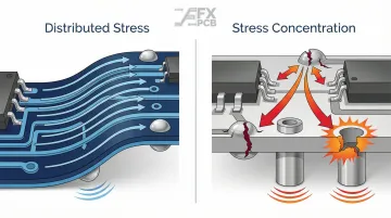
The low stiffness and mass of flex circuits absorb shock and vibration far better than rigid boards. Polyimide substrates withstand significant strain without cracking—particularly valuable in automotive under-hood electronics, industrial machinery sensors, and military equipment where vibration and mechanical shock are constant.
Why this matters: Rigid PCBs mounted with standoffs can crack at solder joints or mounting holes under repeated vibration. Flex circuits distribute mechanical stress across the entire structure rather than concentrating it at rigid points.
Enhanced Thermal Performance
Polyimide substrates maintain physical and electrical properties from -269°C to 400°C, far exceeding FR-4's typical 130-140°C glass transition temperature. This extreme temperature survivability makes flex PCBs ideal for automotive under-hood applications (where ambient temperatures exceed 125°C), industrial process control, and aerospace electronics.
Important nuance: While polyimide survives extreme temperatures, its thermal conductivity (0.12 W/m·K) is actually lower than FR-4 (0.25-0.4 W/m·K). Polyimide excels at withstanding high temperatures, not conducting heat away. For applications requiring heat dissipation, metal-core PCBs or thermal vias remain necessary.
Design Flexibility for 3D Packaging
Flex circuits enable electrical connections in three dimensions between components not on the same plane. Rather than using multiple rigid boards with connectors, designers can fold a single flex circuit into a 3D shape—wrapping around cylindrical housings, conforming to curved enclosures, or folding accordion-style to fit into compact spaces.
This opens up form factors that rigid boards simply can't achieve: medical probes with electronics wrapped around a cylindrical shaft, curved automotive dashboard displays, and rollable screens in foldable consumer devices.
Challenges and Limitations to Consider
Higher Upfront Cost
Flexible PCBs cost 3-8x more than comparable rigid FR-4 boards, driven by multiple factors:
- Expensive materials: Polyimide costs up to 30x more than FR-4 per square foot ($6-60 vs. ~$2)
- Complex manufacturing: 40-50 process steps vs. 20-30 for rigid boards, including specialized coverlay alignment, laser cutting, and stiffener lamination
- Low panel utilization: Irregular flex shapes nest poorly on manufacturing panels, wasting expensive polyimide material
- Lower yields: Polyimide's dimensional instability (shrinking/stretching with humidity) causes layer registration issues, reducing manufacturing yield to 80-90% vs. >95% for rigid boards
Cost mitigation strategies: Minimizing layer count (moving from 2 to 4 layers increases costs 35-40%), using standard copper weights, and optimizing board shape for panel utilization all reduce costs. Free DFM analysis from an experienced manufacturer like SFX PCB can also prevent expensive redesigns before fabrication starts.
Design Complexity—Bending Rules and Via Placement
Flexible PCBs demand strict design rules that don't apply to rigid boards:
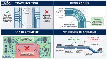
- Trace routing: Traces routed perpendicular to the bend axis experience less strain than parallel traces. Curved or teardrop routing in bend zones distributes stress more evenly than sharp 90-degree corners.
- Via placement: IPC-2223 standards prohibit vias in dynamic flex regions. The plated through-hole creates a stress concentration point that cracks under repeated flexing. Vias must sit in rigid sections or static bend areas only.
- Bend radius: Minimum bend radius is a multiplier of total circuit thickness. IPC-2223 requires 20-40x the thickness for dynamic applications, with some guidelines recommending up to 100x. A 0.2mm flex circuit needs at least a 4mm bend radius.
- Stiffener placement: Stiffeners under heavy components prevent solder joint failure but must stay clear of bend zones to avoid creating stress concentration points.
These rules require thorough DFM review before fabrication. SFX PCB's engineering team offers free DFM analysis to catch issues like vias in flex zones, insufficient bend radii, or improper stiffener placement before they become costly problems.
Manufacturing and Assembly Difficulty
Flex circuits challenge automated assembly equipment designed for flat, rigid boards. The flexible substrate requires specialized handling:
- Pick-and-place complexity: Nozzle height, air pressure, and placement speed must be calibrated because flex boards don't maintain a completely flat surface
- Reflow considerations: Pre-baking at 80-100°C for 4-8 hours removes moisture absorbed during storage, preventing delamination and bubbles during high-temperature reflow
- Testing limitations: AOI produces high false-positive rates on flex PCBs due to non-flat surfaces, requiring X-ray inspection for hidden solder joints
- Rework difficulty: Repair and rework are difficult or impossible once assembled due to the flexible substrate's sensitivity to mechanical stress and heat
Partnering with a manufacturer experienced in flex assembly reduces risk significantly. SFX PCB holds ISO 9001:2015 and IPC-A-610 Class 2/3 certification, with X-ray inspection and functional testing capabilities built specifically for flex circuit production.
Where Flex PCBs Are Used: Industry Applications
Consumer Electronics and Wearables
Flex PCBs are ubiquitous in smartphones, laptops, tablets, digital cameras, smartwatches, and fitness trackers—any device prioritizing compact form factor and light weight. Smartphone camera modules use flex circuits to connect image sensors to main boards through tight, folding paths. Laptop hinges route display signals through flex cables that withstand hundreds of thousands of open/close cycles.
Foldable smartphones represent the most extreme dynamic flex application in consumer electronics. Samsung's Galaxy Z Fold 7 display panel was verified to withstand 500,000 folds, while OPPO's Find N6 achieved 1,000,000 fold cycles using titanium flexion hinges and specialized flex circuits. These devices demand RA copper, adhesiveless constructions, and precise bend radius control to survive years of daily folding.
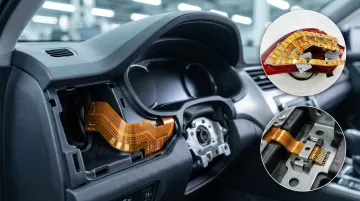
Automotive and Industrial
Flexible circuits replace heavy wire harnesses in automotive instrument clusters, ABS systems, LED headlight modules, and cabin controls. Replacing a standard wire harness with a flex circuit cuts weight by 60-75%, directly improving fuel efficiency and extending electric vehicle range. Flex PCBs bend and fold to fit curved dashboard spaces or angled headlight housings, eliminating bulky connectors and speeding vehicle assembly.
In industrial automation, flex circuits connect sensors and actuators across challenging environments. Rigid-flex designs are particularly effective where traditional wire harnesses fail:
- Robotic joints and conveyor systems subject to continuous motion
- High-vibration process control equipment prone to connector loosening
- Confined enclosures where connector bulk creates assembly or maintenance problems
SFX PCB's IPC-A-610 Class 2/3 certified assemblies are built to the reliability standards automotive and industrial programs demand.
Medical Devices and Aerospace
Flex PCBs enable body-conforming wearable health monitors, implantable neurostimulators, surgical tools, and diagnostic equipment. The thin, flexible form factor lets electronics wrap around curved anatomical structures or fold into compact catheter assemblies.
Critical regulatory requirement: Any FPCB contacting patients must undergo ISO 10993 biocompatibility testing for cytotoxicity, sensitization, and irritation. Material selection is equally constrained:
- Medical-grade polyimide or Liquid Crystal Polymer (LCP) is required for permanent implants — standard polyimide is not approved for long-term human implantation
- LCP's ultra-low moisture absorption (0.04% vs. polyimide's 2.8%) prevents signal degradation inside the body over years of operation
SFX PCB holds ISO 13485 certification for medical device manufacturing, ensuring compliance with medical quality management system requirements throughout the production process.
In aerospace and defense, rigid-flex designs eliminate connector-induced failure points in high-vibration environments such as aircraft avionics, satellite systems, and military munitions. The 20-60% weight reduction and improved shock resistance make rigid-flex the go-to choice for mission-critical platforms where every gram counts and a failed connector is not an option.
Frequently Asked Questions
What is a flexible printed circuit board?
A flexible PCB is a circuit board built on a bendable polymer substrate—typically polyimide—that allows it to flex, fold, or conform to three-dimensional shapes. Unlike rigid PCBs that use stiff FR-4 fiberglass, flexible circuits can bend around corners, fit into tight spaces, and withstand dynamic flexing in applications like foldable phones or wearable sensors.
Are flexible printed circuit boards more expensive than rigid PCBs?
Yes, flex PCBs cost 3-8x more upfront due to expensive polyimide materials, complex manufacturing processes, and lower panel utilization. However, total system cost can be lower when accounting for eliminated connectors, reduced assembly time, lighter weight, and fewer failure points. This is especially true in designs replacing bulky wire harnesses or multi-board assemblies.
What materials are used in flexible PCBs?
Flexible PCBs are built from four layers: a polyimide or PET substrate, copper foil conductor, bonding adhesive, and a protective coverlay film. Polyimide handles temperatures up to 400°C and suits most demanding applications, while PET works for low-temperature, cost-sensitive designs.
What is the difference between a flex PCB and a rigid-flex PCB?
A flex PCB is entirely flexible throughout its structure, designed to bend or fold. A rigid-flex PCB combines rigid FR-4 sections (for component mounting) and flexible polyimide sections (for interconnection) laminated into a single integrated structure, eliminating connectors between boards while providing stable platforms for components.
How many layers can a flexible PCB have?
Flexible PCBs range from single-layer to multilayer configurations with 10+ conductor layers. Single and double-sided designs are most common and cost-effective. Each additional layer increases routing density but reduces flexibility and raises cost, so complexity and bendability must be balanced against each other.
What industries commonly use flexible printed circuit boards?
Flexible PCBs are widely used in consumer electronics (smartphones, wearables), automotive (instrument clusters, LED lighting), medical devices (wearable monitors, implantables), industrial automation, and aerospace/defense. They suit any design that demands compact packaging, light weight, or non-planar circuit routing.