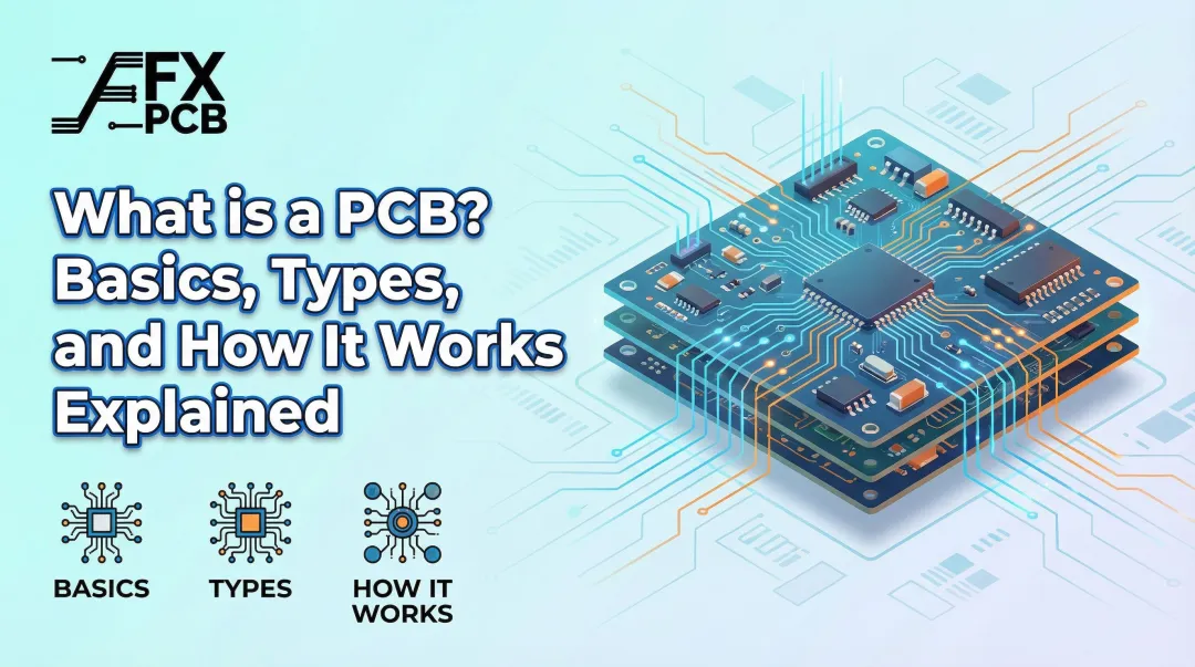
A printed circuit board (PCB) is the physical platform that connects and supports virtually all electronic components in modern electronics. Understanding PCB basics is the essential first step for anyone entering electronics design, procurement, or manufacturing—whether you're an engineer prototyping a new product, a startup founder launching hardware, or a procurement professional sourcing reliable manufacturing partners.
This guide covers what a PCB is and how it works, its key components, the different types available, materials used in fabrication, where PCBs are found across industries, and what you need to know before moving from design to production.
Key Takeaways
- A PCB is a flat, non-conductive board with copper pathways that mechanically support and electrically connect electronic components
- PCBs come in multiple types: single-sided, double-sided, multilayer, flexible, and rigid-flex—each suited for different applications
- Core PCB components include copper traces, pads, vias, solder mask, and silkscreen
- PCBs power nearly every electronics category, from consumer devices and automotive systems to medical and industrial equipment
- A bare PCB becomes functional only once components are soldered onto it—that finished product is called a PCBA (Printed Circuit Board Assembly)
What Is a PCB? Definition and How It Works
A printed circuit board (PCB) is a laminated structure of non-conductive substrate material (typically fiberglass or epoxy) with conductive copper layers etched or printed onto its surface to create pathways for electrical current between components. PCBs serve two critical functions simultaneously: they act as a mechanical support structure holding resistors, capacitors, ICs, and connectors in place, and as an electrical interconnect system routing current precisely between those components.
PCB vs. PCBA: Understanding the Difference
A bare PCB is the unpopulated board fresh from fabrication—just the substrate, copper traces, and protective coatings. A PCBA (Printed Circuit Board Assembly) is the board after electronic components have been soldered onto it. Neither the PCBA nor the final product can exist without the bare PCB as its foundation. When sourcing manufacturing services, keep this distinction in mind: PCB fabrication produces the bare board, while PCBA services handle component placement and soldering.
Why PCBs Replaced Point-to-Point Wiring
Before PCBs became standard, electronic systems relied on labor-intensive point-to-point wiring where individual wires connected each component. This method was slow, error-prone, and impossible to scale. The transition to printed circuits (pioneered by Paul Eisler in the 1930s and scaled during World War II) transformed electronics manufacturing by:
- Reducing circuit size dramatically
- Enabling mass production automation
- Improving reliability through standardized manufacturing
- Cutting manufacturing costs by orders of magnitude
These advantages made modern electronics scalable from prototype to high-volume production runs, enabling the consumer electronics revolution.
The Scale of the PCB Industry
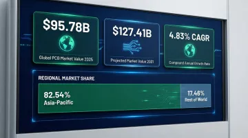
The PCB industry is a massive global engine. According to Mordor Intelligence, the global PCB market is projected to reach $127.41 billion by 2031, growing at a 4.83% CAGR from $95.78 billion in 2025. Asia-Pacific dominates production, manufacturing 82.54% of global PCB output. For engineers and product teams, this means PCB supply chains, manufacturing standards, and sourcing decisions carry real weight at every stage of development.
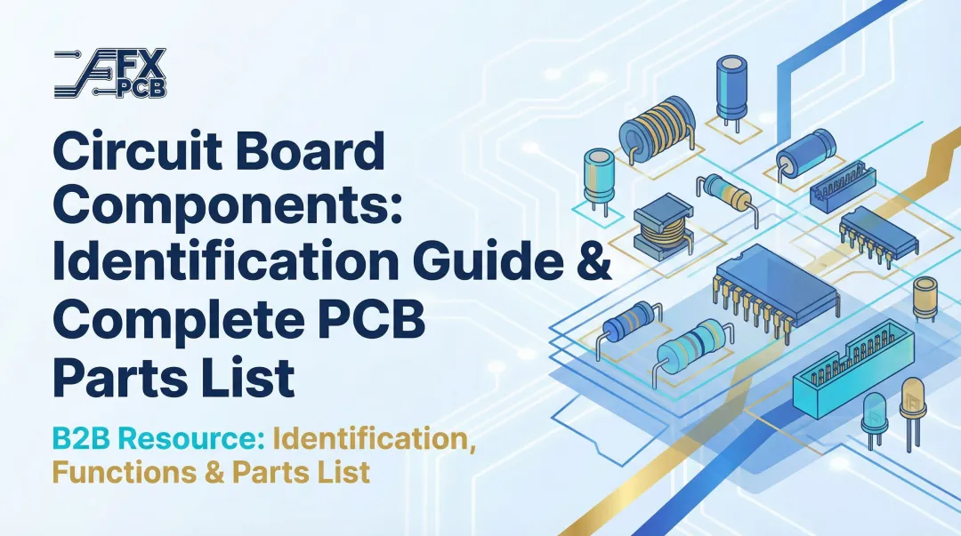
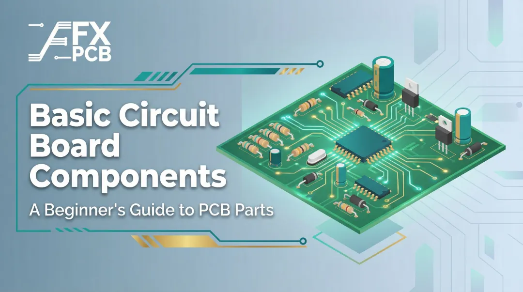
Key Components of a Printed Circuit Board
A PCB's function depends on several standardized components, each playing a distinct role in signal routing, protection, and assembly:
Copper Traces
Traces are the narrow copper pathways etched into the board that function as the "wires" of a PCB. They carry electrical signals and power between components. Trace width directly affects current capacity and signal integrity—wider traces handle more current, while narrower traces save space but require careful thermal management.
For decades, engineers sized traces using the IPC-2221 standard from the 1950s. In 2009, IPC released IPC-2152, which officially superseded those older charts.
Extensive empirical testing showed that internal traces can carry more current than previously believed, largely due to heat-sinking effects from nearby copper planes. Engineering teams should update their EDA tools to IPC-2152 to safely reduce trace widths and recover board real estate.
Pads and Holes
Pads are the exposed metal areas where component leads are soldered. Two types exist:
- Through-hole pads: For components with leads that pass through the board
- Surface mount pads: For components placed directly on the board surface
Vias are drilled, copper-plated channels that create electrical connections between different copper layers. They come in three configurations: through-vias (extending through the entire board), blind vias (extending from an outer layer partway through), and buried vias (contained entirely within inner layers).
Solder Mask
The solder mask is the protective polymer coating—most often green, though other colors exist—that covers the copper traces. It serves multiple critical functions:
- Prevents copper oxidation
- Reduces risk of solder bridges between traces
- Protects the board from moisture and contamination
- Provides electrical insulation
Silkscreen
The silkscreen layer consists of printed text and symbols on the board surface: component reference designators (R1, C5, U3), polarity markers, test point labels, and assembly instructions. This layer guides assembly technicians and makes troubleshooting far easier during development and repair.
Substrate (Base Material)
All these layers sit on top of—or are laminated between—a non-conductive base material. The most common substrate is FR-4, a woven fiberglass cloth impregnated with epoxy resin. FR-4 provides structural rigidity, electrical insulation, good thermal properties, and fire retardancy, making it the default for most commercial and industrial PCBs.
Types of PCBs: From Single-Layer to Flex
PCBs come in multiple configurations based on layer count and physical form.
By Number of Copper Layers
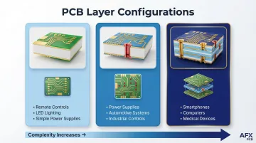
The three main layer configurations each suit a different complexity level:
| Type | Structure | Common Applications |
|---|---|---|
| Single-Sided | One copper layer, one side | Remote controls, LED lighting, simple power supplies |
| Double-Sided | Copper on both sides, connected by vias | Power supplies, automotive electronics, industrial controls |
| Multilayer | 3+ copper layers, insulating material between each | Smartphones, computers, medical devices, industrial equipment |
According to Mordor Intelligence, standard multilayer boards held 29.64% of market share in 2025. Additional copper layers enable:
- More complex signal routing
- Dedicated ground and power planes for better signal integrity
- Significantly reduced board size
- Enhanced electromagnetic shielding
SFX PCB fabricates multilayer boards from 4 to 68 layers, supporting everything from basic 4-layer designs to complex HDI applications.
By Physical Form
Rigid PCBs are structurally stiff boards used in the vast majority of electronics. They provide excellent mechanical stability and are the most economical option for most applications.
Flexible PCBs are made on thin polyimide film that can bend and fold. Flexible circuits are expanding at a 5.39% CAGR, driven by wearables, foldable smartphones, cameras, and medical devices where space constraints and dynamic movement are factors.
Rigid-Flex PCBs combine rigid and flexible sections in one board. Aerospace, military, and compact IoT applications favor them for vibration resistance and three-dimensional packaging — benefits that justify the 30-50% cost premium over standard rigid boards.
Specialty Types
HDI (High-Density Interconnect) PCBs are defined by IPC-2226 as having higher wiring density per unit area than conventional PCBs. Their defining feature is the microvia: a blind structure with a maximum aspect ratio of 1:1 and finished hole diameters typically from 75 µm to 150 µm. HDI boards are the go-to option for premium smartphones, 5G infrastructure, and medical implantables.
IMS (Insulated Metal Substrate) or Metal Core PCBs use aluminum or copper base plates for superior heat dissipation. Ventec's thermal management materials offer thermal conductivities up to 4.2 W/m·K and higher, making them ideal for LED arrays, automotive power electronics, and high-power applications.
Choosing the right PCB type comes down to your application's complexity, thermal requirements, and physical constraints — factors covered in the design considerations section below.
What Are PCBs Made Of? Materials and Substrate Overview
FR-4: The Industry Standard
FR-4 is the most widely used PCB substrate—a woven fiberglass cloth impregnated with epoxy resin. The "FR" stands for "flame retardant." Key properties include:
- Good electrical insulation
- Low moisture absorption
- Mechanical rigidity
- UL 94 V-0 flammability rating
The UL 94 V-0 rating indicates that the material was tested in a vertical position and self-extinguished within a specified time without dripping flaming particles—a critical safety standard.
Specifying generic "FR-4" is no longer sufficient for demanding applications. Engineers must specify exact laminate SKUs based on Glass Transition Temperature (Tg), Dielectric Constant (Dk), and other properties. For example, Isola IS410 offers a Tg of 180°C and Dk of 3.97 @ 2 GHz with UL 94 V-0 certification.
Copper Thickness Specifications
Copper thickness is measured in ounces per square foot (oz/ft²). 1 oz/ft² translates to approximately 35 µm or 1.37 mils—the standard for most boards. Heavy copper boards (3+ oz/ft²) are used for high-current or power electronics like automotive systems and power supplies, where they handle significant current without overheating. SFX PCB offers copper weights from 1 oz to 20 oz, supporting everything from standard digital circuits to high-power applications.
Alternative Substrates for Specialized Applications
When FR-4 can't meet the demands of an application, engineers turn to specialized substrates. The three most common alternatives each solve a different problem:
| Substrate | Best For | Key Advantage | Example |
|---|---|---|---|
| Polyimide | Flexible circuits, wearables, aerospace wiring | High Tg (up to 260°C), survives dynamic bend cycles | DuPont Kapton |
| IMS / Metal-Core | Power electronics, high-intensity LEDs | Thermal conductivity of 4.2 W/m·K or higher | Ventec VT-4B5 |
| PTFE / Low-Loss | RF, microwave, 5G, radar | Tight Dk control, low signal loss at high frequencies | Rogers RO4350B |
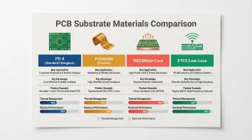
Metal-core boards use aluminum or copper base plates bonded to thermal prepreg, making them the go-to choice wherever heat dissipation is the primary design constraint. PTFE composites like RO4350B are critical for telecommunications infrastructure where signal integrity at high frequencies cannot be compromised.
Where PCBs Are Used: Applications Across Industries
PCBs are the foundational component of nearly every electronic product made today. Different industries demand unique performance, reliability, and certification requirements.
Consumer Electronics
Smartphones, laptops, televisions, gaming consoles, and home appliances all depend on PCBs. These applications typically require cost-effective multilayer boards with moderate reliability standards (IPC Class 2).
Automotive Systems
The global automotive PCB market was estimated at $9.79 billion in 2023 and is projected to reach $14.09 billion by 2030 (5.7% CAGR). Key growth drivers include:
- Advanced driver-assistance systems (ADAS)
- Electric vehicle powertrains
- Engine control units
- Battery management systems
Automotive PCBs often require multilayer and heavy-copper designs to handle high currents and harsh operating environments.
Medical Devices
The medical device PCB market is projected to reach $13.32 billion by 2025, exhibiting a 6.9% CAGR. Applications include patient monitors, imaging equipment, implantables, and wearable health devices.
Medical PCBs demand miniaturization, biocompatibility, and strict adherence to IPC Class 3 standards. ISO 13485 certification is the baseline requirement — SFX PCB carries this certification, which covers full material traceability and quality documentation on every medical-grade order.
Industrial Automation
Industrial environments place some of the toughest demands on PCB hardware. Common applications include:
- PLCs (programmable logic controllers) and motor drives
- Industrial robotics and automated assembly systems
- Environmental sensors and process control modules
These boards are typically designed for extended service life with conformal coating or waterproofing protection against moisture, dust, and mechanical vibration.
Telecommunications
The 5G PCB market is forecast to grow at an 8.0% CAGR, reaching $15.3 billion in 2031 from $10.4 billion in 2026. 5G base stations require millimeter-wave frequencies, driving demand for advanced HDI PCBs and low-loss substrates like PTFE laminates to maintain signal integrity at high frequencies.
Each of these industries maps to a different tier of manufacturing quality. That's where IPC-A-610 classification comes in.
IPC-A-610 Acceptability Classes
The IPC-A-610 standard categorizes products into three classes based on reliability requirements:
- Class 1 (General): Function is the major requirement; cosmetic imperfections acceptable. Used in consumer toys and basic electronics.
- Class 2 (Dedicated Service): Continued performance and extended life required; uninterrupted service desired but not critical. Used in laptops, HVAC controls, and televisions.
- Class 3 (High Performance): Performance-on-demand is critical; equipment downtime cannot be tolerated. Used in aerospace, military, and life-support medical equipment.
| Requirement | Class 2 | Class 3 |
|---|---|---|
| Hole-to-pad registration | Moderate tolerance | Near-perfect alignment |
| Minimum barrel fill | 50% | 75% |
| Cosmetic imperfections | Limited, acceptable | Not permitted |
| Typical cost impact | Standard | Higher manufacturing time and cost |
Specifying Class 3 for a Class 2 product adds cost and lead time without meaningful reliability gains — getting this right at the design stage matters.
From Design to Manufacture: PCB Design Basics
The Standard PCB Design Workflow
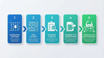
Every PCB moves through the same core sequence, from first schematic to finished board:
- Schematic Capture — Draw the logical circuit diagram defining which components connect to which
- PCB Layout — Translate the schematic into a physical board by placing components and routing copper traces
- DFM/DRC Checks — Review design for manufacturability and rule violations
- Gerber File Generation — Create industry-standard fabrication output files
- Fabrication & Assembly — Send files to manufacturer for production
Decisions made at each stage directly affect cost, yield, and signal performance — which is why the design choices below matter before you ever submit a file.
Critical Design Considerations
Four variables drive the majority of design-to-manufacture problems:
- Trace width and spacing — Determines current capacity and signal integrity; use IPC-2152 for accurate current-carrying calculations
- Layer stackup — Proper stackup on multilayer boards controls impedance and power distribution across the board
- Component placement — Group related components, respect thermal zones, and minimize trace lengths for high-speed signals
- Via type — Through-hole vias are standard; blind and buried vias unlock HDI density but add cost
The Economics of Design for Manufacturability (DFM)
Design for Manufacturability (DFM) is the critical bridge between a functional design and a producible, cost-efficient board. A DFM review checks for:
- Minimum trace widths and spacing
- Drill-to-copper clearances
- Pad size adequacy
- Annular ring specifications
- Manufacturability constraints
According to a NASA study, finding and fixing a problem after delivery can be upwards of 100 times more expensive than finding it during early design phases. Late corrections involve extensive revalidation, scrap, and formal change approvals.
SFX PCB provides free DFM analysis on every order, helping customers catch costly design errors before production starts. The SFX PCB engineering team typically responds within 12 hours of receiving new PCB files. Feedback covers specific issues — insufficient spacing, annular ring problems, trace width violations — before they become manufacturing delays.
Fabrication Outputs: The Gerber Standard
The Gerber file format is the de facto open standard for PCB design data transfer. Standard Gerber (RS-274-D) is technically obsolete and was revoked because it lacked the imaging primitives needed to unequivocally transfer information.
The modern standard is Extended Gerber (RS-274X / X2 / X3). Released in 2014, Gerber X2 adds structured metadata via attributes. For example, the .AperFunction attribute explicitly tells the CAM software whether a pad is an SMD pad, a via pad, or a fiducial—eliminating manual guesswork for the fabricator and reducing errors.
Frequently Asked Questions
What is a PCB?
A PCB (printed circuit board) is a flat board made of non-conductive substrate material with etched copper pathways that mechanically support and electrically connect electronic components. It serves as the backbone of virtually every electronic device, from smartphones to medical equipment.
What are PCBs used for?
PCBs power and connect the electronics in nearly every modern device. Key industries include consumer electronics, automotive, medical devices, telecommunications, aerospace, and industrial automation — each with its own performance and reliability requirements.
What is the difference between a PCB and a PCBA?
A PCB is the bare, unpopulated board fresh from fabrication—just the substrate, copper traces, and protective coatings. A PCBA (Printed Circuit Board Assembly) is the board after electronic components have been soldered onto it. The PCBA is what actually performs a circuit function in a final product.
What materials are PCBs made of?
Most PCBs use FR-4 fiberglass-epoxy as the base substrate, with copper layers for conductors, solder mask for protection, and silkscreen for labeling. Specialized applications may use polyimide (for flexible circuits), aluminum core (for thermal management), or PTFE-based materials (for high-frequency RF applications).
What are the different types of PCBs?
PCBs are classified by layer count (single-sided, double-sided, or multilayer) and physical form (rigid, flexible, or rigid-flex). Specialty types include HDI boards for miniaturized devices and metal core boards for high-power thermal management.
How long does it take to manufacture a PCB?
Lead times vary based on board complexity and quantity. Standard prototypes are typically fabricated in 3–5 business days. For example, SFX PCB offers assembled boards from 24 hours once all parts are available, with typical PCBA turnkey delivery in 1–2 weeks.