Not all circuit boards are created equal. Single-layer boards served simple electronics well for decades, but today's demanding applications—high-speed data transmission, complex signal processing, miniaturized medical devices—require something fundamentally more capable. Enter the multilayer PCB: the engineering solution that makes high-density, high-performance electronics possible.
This article explains what a multilayer PCB is, how it's built, how it compares to simpler alternatives, and why understanding it matters whether you're an engineer designing the next generation of products, a product developer evaluating manufacturing options, or a sourcing manager selecting the right PCB partner.
TLDR:
- Multilayer PCBs stack three or more conductive copper layers separated by insulating material, enabling far greater routing density than single or double-sided boards
- They deliver superior signal integrity and EMI control through dedicated ground and power planes—essential for high-speed digital, RF, and automotive applications
- Cost scales exponentially with layer count (a 4-layer board costs 3-4× more than 2-layer), but volume production dramatically reduces per-unit pricing
- The global multilayer PCB market is projected to reach $116.1 billion by 2032, driven by 5G, ADAS, IoT, and advanced computing demands
- Choosing a manufacturer with ISO9001, ISO13485, and IPC-A-610 certifications plus free DFM analysis prevents costly errors before lamination
What Is a Multilayer PCB?
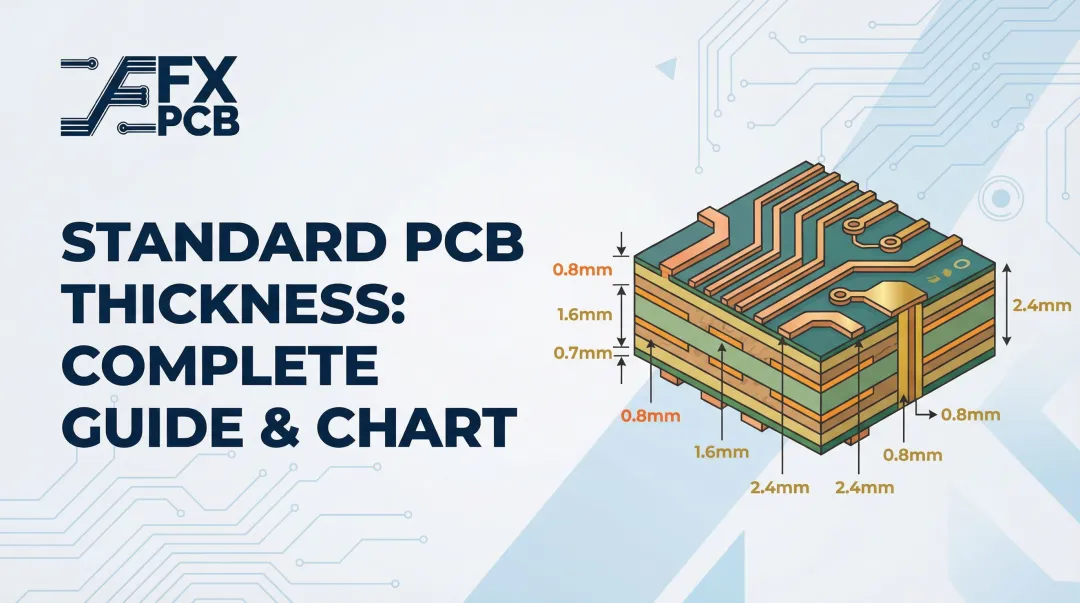
A multilayer PCB is a printed circuit board made up of three or more conductive copper layers separated by insulating material (prepreg and core), laminated together under heat and pressure into a single solid structure. The "multi" in multilayer refers specifically to the stacking of internal conductive layers beyond the two surfaces of a standard double-sided board.
While three conductive layers technically qualify as multilayer, designers overwhelmingly use four or more layers—and almost always even numbers. Why? Odd-layer counts introduce serious manufacturing challenges. Asymmetrical lamination causes severe thermal warpage and bow/twist defects during cooling, as the imbalanced materials shrink and expand at different rates. Fabricators actively avoid odd-layer configurations, recommending even-layer designs (4, 6, 8 layers) with symmetrical stackups to ensure mechanical stability and high yields.
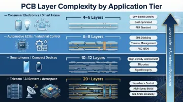
Layer Count Benchmarks by Application
Layer counts scale directly with device complexity, pin density, and signal integrity requirements:
| Product Category | Typical Layer Count | Design Drivers |
|---|---|---|
| Consumer Electronics / Smart Home | 4-6 layers | Basic microcontrollers, cost-sensitive designs, moderate routing |
| Automotive ECUs / Industrial | 6-8 layers | EMI control, high-temperature materials, reliable power distribution |
| Smartphones / Compact Devices | 10-12 layers | High-Density Interconnect (HDI), fine-pitch BGAs, extreme space constraints |
| Telecom / AI Servers / Aerospace | 20+ layers | 112G/224G SerDes channels, massive routing density, strict impedance control |
Most commercial applications use 4 to 8 layers. Smartphones and compact devices may push to 10-12 layers. Highly complex systems in aerospace, defense, or server infrastructure can exceed 20 or even 32 layers.Layer count has no fixed ceiling — it scales with application need. SFX PCB's manufacturing capabilities extend up to 68 layers for rigid FR4 boards, covering even the most demanding high-density designs.
The Role of Different Layer Types
What makes multilayer PCBs electrically superior isn't just stacking copper — it's the intentional assignment of layer functions:
- Signal layers route traces carrying data and control signals between components
- Ground planes provide continuous, low-impedance return paths for signals and act as electromagnetic shields
- Power planes distribute stable voltage across the board with minimal voltage drop
This deliberate layer architecture is what produces measurable improvements in signal integrity, EMI suppression, and power stability — outcomes that simply adding more copper cannot achieve.
That architecture didn't appear by accident. Multilayer PCBs emerged in the 1960s and saw widespread adoption through the 1970s and 1980s as a direct engineering response to a fundamental problem: single- and double-sided boards hit functional limits as component density grew. Noise, crosstalk, and routing constraints could no longer be solved on two layers. The 1961 patenting of hole plating technology enabled internal layers to be interconnected, unlocking the multilayer architecture that powers virtually all modern electronics.
How Multilayer PCBs Are Built
Raw Materials: Cores, Prepreg, and Copper
Multilayer PCBs are constructed by bonding alternating layers of two key materials:
- Core: Fully cured laminate with copper foil already bonded to one or both sides. The core provides structural rigidity and serves as the foundation for inner-layer circuitry.
- Prepreg (B-stage resin-impregnated fiberglass): Partially cured resin sheets that act as the bonding and insulating material between cores during lamination.
The most common base material is FR-4 (Flame Retardant 4), a glass-reinforced epoxy laminate offering a good balance of cost, electrical properties, and mechanical strength. For high-performance applications, specialized materials deliver tighter electrical or thermal properties:
| Material Type | Glass Transition (Tg) | Dielectric Constant (Dk) | Dissipation Factor (Df) | Typical Applications |
|---|---|---|---|---|
| Standard FR-4 | ~130°C | 4.3 @ 10GHz | 0.020 @ 10GHz | General commercial electronics |
| High-Tg FR-4 (e.g., Isola 370HR) | 180°C | 4.04 @ 2GHz | 0.0210 @ 2GHz | Automotive, industrial, LED |
| Hydrocarbon Ceramic (e.g., Rogers RO4835) | 280°C | 3.48 @ 10GHz | 0.0037 @ 10GHz | 5G telecom, automotive radar, high-speed digital |
| Polyimide (e.g., Arlon 85N) | ≥250°C | 4.1 @ 1MHz | ~0.01 @ 10GHz | Aerospace, defense, extreme environments |
Material selection comes down to operating frequency and thermal environment. Standard FR-4 handles most commercial applications, but once clock speeds or RF frequencies climb, its higher Dk and Df values introduce signal loss that specialized laminates are specifically engineered to avoid.
The Lamination Process
All layers — cores with etched circuitry and prepreg sheets — are aligned precisely using registration holes, then stacked in the correct order. This stack is placed in a hydraulic press where heat and pressure melt the prepreg resin, which flows and cures to bond everything into a single solid board.
Processing parameters vary by laminate. For Isola FR408HR, for instance, the cycle requires:
- Vacuum time: 30 minutes
- Cure temperature: 188–202°C
- Pressure: 300–350 PSI for 130–160 minutes
Once laminated, the process is irreversible. Inner layers cannot be accessed or reworked, so any design errors are locked in permanently. Running a thorough DFM check before lamination is the only realistic way to catch those errors.
High-Density Interconnect (HDI) boards require sequential lamination, where sub-assemblies are pressed, drilled, and plated multiple times. This significantly increases fabrication time and cost but enables the fine-pitch routing and microvia structures essential for compact, high-performance devices.
Electrical Interconnection: Vias
Layers are electrically interconnected using vias — plated holes that conduct signals between layers. IPC standards define several distinct via types:
- Through-hole vias (PTH): Drill through the entire board, connecting all layers. Simple and cost-effective, but consume routing space on every layer.
- Blind vias: Connect an outer layer to one or more inner layers without passing through the entire board. Visible from only one side.
- Buried vias: Connect internal layers only and are completely hidden from external surfaces.
- Microvias: Defined by IPC-T-50 as blind structures with a maximum aspect ratio of 1:1 and a depth not exceeding 0.25mm. Typically laser-drilled (down to 4mil/0.10mm), microvias are essential for HDI designs but require complex manufacturing steps including desmear, electroless copper deposition, and electroplating to achieve void-free copper filling.
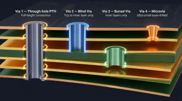
Blind and buried vias save routing space and are essential for high-density designs, but add manufacturing complexity and cost (typically 10-30% premium). SFX PCB supports blind and buried vias on their 6-layer and higher configurations, with laser drilling capabilities down to 0.10mm (4mil) for low-volume production.
Multilayer PCB vs. Single and Double-Layer PCBs
Routing Density and BGA Escape
A single-layer PCB is limited by its surface area—if you need more connections, you need a bigger board. A double-sided PCB adds a second routing surface. A multilayer PCB multiplies available routing space by adding internal layers without increasing the footprint. This is what allows high-density chips—like fine-pitch Ball Grid Arrays (BGAs)—to be used on compact boards.
According to IPC-2226 guidelines, BGAs with a 0.8mm pitch can typically be routed using a Type I HDI stackup (1+N+1), while 0.5mm pitch BGAs require Type III HDI (2+N+2) with stacked or staggered microvias. Standard through-hole routing simply fails when BGA pitches drop below 0.8mm, forcing a transition to multilayer HDI structures.
Size and Weight Impact
Multilayer PCBs replace what would otherwise require multiple interconnected single- or double-sided boards. By integrating everything into one compact board, the final assembly is smaller and lighter—a critical advantage for mobile devices, wearables, and aerospace applications where space and weight are tightly constrained.
Electrical Performance: EMI Shielding and Signal Integrity
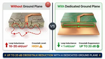
Single and double-layer boards lack dedicated ground and power planes, making them susceptible to noise, signal interference, and electromagnetic interference (EMI). Every signal requires a return path; without a continuous ground plane, return currents wander, creating large loop areas that act as antennas.
A solid ground plane provides a low-impedance return path directly beneath the signal trace, reducing loop inductance to below 1 nH/cm²—compared to 10–20 nH/cm² for routed ground traces. Placing a ground plane between two signal layers (stripline configuration) can reduce crosstalk by up to 20 dB.
Two quantified gains from proper ground plane placement:
- Loop inductance: drops from 10–20 nH/cm² to below 1 nH/cm²
- Crosstalk suppression: up to 20 dB reduction in stripline configuration
For high-speed digital signals, controlled impedance is essential to prevent reflections and signal distortion. Transmission line effects kick in when a trace exceeds 1/10th of the signal's wavelength—at 1 GHz, that's just 30mm.
Multilayer PCBs let designers precisely control trace width, copper thickness, and dielectric spacing relative to a continuous reference plane, ensuring adherence to target impedances (such as 50Ω single-ended). SFX PCB maintains impedance control tolerance of ±10% across our multilayer offerings.
When to Choose Multilayer
Single/double-layer boards remain cost-effective and entirely appropriate for:
- Simple, low-speed applications
- Basic sensors and LED drivers
- Simple controls and power supplies
- Cost-sensitive consumer products
Multilayer PCBs become necessary when the design demands:
- High component density (fine-pitch BGAs, compact footprints)
- Controlled impedance for high-speed signals (>100 MHz)
- Strong EMI suppression and signal integrity
- Miniaturization for portable or wearable devices
- Automotive, medical, or industrial reliability requirements
Key Benefits — and Trade-offs to Know
Advantages Worth Understanding
Compact, High-Density Design
Because routing expands vertically through layers rather than horizontally across a larger board, multilayer PCBs achieve far higher component density in a smaller footprint. This vertical scaling is what enables the miniaturization trend driving modern electronics—from smartphones with 10-12 layer boards to wearables and IoT sensors.
Improved Signal Integrity and EMI Control
Dedicated ground and power planes act as electromagnetic shields and provide stable return paths for high-speed signals, reducing crosstalk and radiated emissions. For any high-speed digital or RF design, these continuous reference planes are what keep signal integrity intact as clock speeds and data rates climb.
Single Connection Point and Cleaner Design
Rather than connecting multiple separate PCBs with cables or connectors, a multilayer PCB consolidates everything into a single board with a single interface. This reduces potential failure points, simplifies assembly, and improves overall product reliability.
Those advantages come with real costs—both in budget and in schedule. Here's what to plan for.
Trade-offs to Plan For
Higher Upfront Cost
Multilayer PCBs require more materials, more manufacturing steps, and greater design effort than single-layer equivalents. Each additional layer adds disproportionately to cost—a 4-layer board typically runs 3 to 4 times the price of a 2-layer board. Moving from 6 layers to 8 layers generally increases costs by 30–40%. Including blind or buried vias adds another 10-30% to total PCB cost.
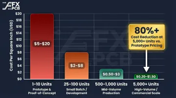
However, per-unit economics change dramatically at higher production volumes:
| Quantity Range | Typical Cost (per sq inch) | Best For |
|---|---|---|
| 1-10 pieces | $5.00 – $20.00 | Prototyping, testing |
| 25-100 pieces | $2.00 – $8.00 | Small batch production |
| 500-1000 pieces | $0.50 – $3.00 | Medium production runs |
| 5000+ pieces | $0.20 – $1.50 | High volume production |
At 5000+ units, per-square-inch costs drop by over 80% compared to prototype runs. If your design is stable, batching orders at the 500+ tier is often the fastest path to margin improvement.
Longer Design and Production Time
The additional complexity in layout—impedance planning, layer stack-up design, via strategy—and in manufacturing (multiple lamination cycles, alignment precision, testing) means longer lead times. Designers must account for this in project timelines, especially at the prototype stage.
Typical turnaround benchmarks to plan around:
- Quick-turn (domestic): 2-4 layer boards in 24–48 hours; 6-8+ layer boards in 3–7 days, usually at a 30–70% price premium
- Standard volume facilities: 5–10 days for standard multilayers; 10–20 days for complex HDI or high-layer-count boards
Where Multilayer PCBs Are Used
The global multilayer PCB market was valued at $71 billion in 2023 and is projected to reach $116.1 billion by 2032, growing at a CAGR of 5.5%. The 4 to 6 layer segment currently dominates in terms of revenue, but the 6+ layer segment is growing fastest due to increasing complexity in end-user devices.
Primary Industries and Applications
Each major industry has distinct requirements that push multilayer PCB complexity in different directions:
- Consumer Electronics: iPhone X teardowns show double-stacked SLP logic boards with microvias and trace widths down to 10-15 µm — packing maximum performance into minimal space.
- Medical Devices: Implantable devices like Medtronic pacemakers use compact multilayer boards built to operate reliably for 6-10 years inside the body. Imaging equipment and monitors depend on them for precise signal processing and noise immunity.
- Automotive: ECUs and ADAS sensors typically use 6-10 layers to isolate high-speed digital signals from analog sensor inputs while handling high thermal loads. Magna Electronics ADAS controllers integrate Texas Instruments processors across multiple dedicated layers.
- Telecommunications: 5G base stations demand high-frequency performance at scale. Huawei BBU5900 baseband units use 12- to 24-layer hybrid stackups — combining standard FR-4 with low-loss Rogers materials to handle 28–39 GHz frequencies.
- Aerospace and Defense: These applications specify 20+ layer boards with advanced materials and rigorous testing protocols to withstand temperature extremes, vibration, and radiation exposure.

The common thread is high performance within constrained physical space or harsh operating environments. As IoT sensors, electric vehicles, and implantable medical tech push into mainstream products, multilayer PCBs are moving well beyond traditionally high-tech industries.
Choosing the Right Multilayer PCB Manufacturer
Experience and Certifications
Look for a manufacturing partner with demonstrated experience in the specific layer counts and materials required for your application. Relevant certifications matter:
- ISO 9001 demonstrates a standardized Quality Management System with consistent processes, rigorous testing, and strict traceability
- ISO 13485 is mandatory for medical device applications, emphasizing risk management, regulatory compliance, and lifecycle traceability
- IPC-A-610 Class 2/3 defines acceptability criteria for printed boards and assemblies, with Class 3 representing high-reliability applications
SFX PCB holds all three certifications alongside ISO14001, backed by over 15 years manufacturing multilayer boards for medical devices, automotive electronics, industrial control systems, and telecom equipment. That experience translates directly into solved problems: signal integrity issues, thermal management constraints, and high-speed routing challenges across demanding applications.
Design for Manufacturability (DFM) Support
DFM support is critical for multilayer boards because design errors—especially in stack-up planning or impedance routing—are impossible to fix after lamination. Key DFM checkpoints include:
| DFM Checkpoint | Manufacturing Rationale |
|---|---|
| Stack-up Symmetry | Layers must be mirrored across the Z-axis median to prevent uneven thermal expansion causing warpage |
| Copper Balance | Copper must be distributed evenly across layers to prevent mechanical stress and plating issues |
| Annular Ring | Pad sizes must account for finished hole diameter plus minimum annular ring to prevent drill breakout |
| Via Aspect Ratios | Mechanical blind vias need ≥1:1 aspect ratio; laser-drilled microvias should be ≤1:1 for uniform plating |
SFX PCB offers free DFM analysis on every order, helping engineers catch issues before production begins. Common catches include trace width violations, inadequate clearances, and impedance mismatches — problems that cost significantly more to fix post-lamination than pre-production.
Scalability from Prototype to Production
Choose a manufacturer who can scale with your project — from prototype to mass production — without switching suppliers. Changing vendors mid-development introduces new process variables, material tolerances, and quality unknowns that can derail a product launch.
SFX PCB supports this scaling across rigid, flexible, and metal-core technologies. Prototypes ship in as little as 24 hours, and the same quality standards apply at every volume — 100% electrical testing, AOI, and X-ray inspection. Transparent quoting typically arrives within 24 hours, with structured NPI procedures that carry your design from first article to full production without rework surprises.
Frequently Asked Questions
What is a multilayer PCB?
A multilayer PCB is a printed circuit board with three or more conductive copper layers separated by insulating material, laminated into a single rigid structure. It's designed to achieve high routing density and improved electrical performance in a compact form factor.
What is the difference between single-layer and multilayer PCBs?
Single-layer PCBs have one conductive layer and are suited for simple, low-cost applications. Multilayer PCBs have three or more layers offering far greater routing density, better EMI shielding, and superior signal integrity—but at higher cost and complexity.
Do 3-layer PCBs exist?
Yes, but they're rarely used. Odd layer counts create lamination challenges (warpage, bow/twist defects) and save little over a 4-layer board, which adds a full reference plane for better electrical performance.
How many layers does a multilayer PCB typically have?
Most commercial applications use 4 to 8 layers. Smartphones and dense consumer devices use up to 12 layers. High-end server, defense, or telecom systems sometimes exceed 20 or more layers depending on routing and performance requirements.
What industries use multilayer PCBs?
Primary industries include consumer electronics, medical devices, automotive, telecommunications, aerospace and defense, and industrial automation—all of which require the compact size, high density, and strong electrical performance that multilayer PCBs provide.
Are multilayer PCBs more expensive than single-layer PCBs?
Yes, due to additional materials, more manufacturing steps, and greater design complexity. Performance gains typically offset the added cost, and at higher production volumes (5,000+ units), per-unit costs decrease significantly.
Ready to move forward with your multilayer PCB project? SFX PCB offers free DFM analysis, ISO-certified manufacturing, and prototype-to-production manufacturing. Contact us at info@sfxpcb.com or call (+1) 5103455000 to discuss your requirements.