

Multilayer PCBs appear constantly in product specs and datasheets, but the engineering rationale behind them is rarely spelled out clearly enough for design teams to make confident architecture decisions. According to Allied Market Research, the global multilayer PCB market was valued at $71 billion in 2023 and is projected to reach $116.1 billion by 2032 — a trajectory that reflects how thoroughly multilayer designs have become the default for complex electronics.
This guide covers what multilayer PCBs actually deliver in engineering terms, where they're applied across demanding industries, and what it takes to move from design intent to a production-ready board.
Key Takeaways
- Multilayer PCBs (3+ conductive layers) resolve signal integrity, density, and size constraints that two-layer boards cannot address in complex designs
- Dedicated internal ground and power planes reduce EMI and control impedance — critical for high-speed digital, RF, and precision analog circuits
- Laminated construction improves thermal performance — ROHM recorded a 30% drop in thermal resistance (50°C/W to 35°C/W) switching from 2-layer to 4-layer in identical package conditions
- Medical, automotive, aerospace, telecom, and industrial automation are the primary industries where multilayer PCBs are standard rather than optional
- Realizing full value requires stackup planning before routing, DFM review before fabrication, and 100% electrical testing on every bare board
What Is a Multilayer PCB?
Per IPC-T-50N, a multilayer board is any printed board with three or more conductor layers — copper foil layers separated by insulating material, laminated together under heat and pressure. Electrical connections between layers are made through vias: plated through-holes, blind vias (connecting an outer layer to one or more inner layers), or buried vias (connecting inner layers without reaching the surface).
The lamination process bonds everything together using prepreg, a glass fiber material with partially cured epoxy that liquefies during the press cycle, then solidifies under controlled pressure. The quality of this process directly affects layer registration, dielectric consistency, and long-term reliability.
Choosing the Right Layer Count
Most commercial designs use 4 to 12 layers, with 4-layer boards being the most common entry point for high-speed or EMI-sensitive work. SFX PCB supports layer counts from 4 to 68 layers across rigid configurations, with 4-layer, 6-layer, and 8-layer boards representing the most frequently specified options.
Layer count should be determined by three factors:
- Routing density: the number of signal traces that must be routed without violating spacing rules
- Impedance control: whether signal layers require adjacent reference planes for consistent characteristic impedance
- EMI and signal isolation: how much physical separation is needed between signal groups to limit crosstalk
Picking a layer count by convention rather than by these constraints is how teams end up either under-specified (and facing re-spins) or over-specified (and paying for layers they don't need).
Key Advantages of Multilayer PCBs
Advantage 1: Superior Signal Integrity and EMI Control
Signal integrity is the ability of an electrical signal to travel through a board without distortion, delay, or interference. In two-layer designs, there's no dedicated return plane — return current has to find its path through whatever ground copper exists on the same layer, which creates longer return loops, higher inductance, and increased radiated emissions.
Multilayer stackups solve this directly. Internal ground planes provide a controlled return path immediately adjacent to every signal layer, reducing loop inductance and keeping EMI in check.
EDN's analysis of ground return planes quantifies the benefit: adding top and bottom ground return planes with perimeter stitching vias every 5mm reduced EMI by 12–18 dB on a test board. In optimized 4-layer designs, every trace sits adjacent to a ground return plane. That structural arrangement is why 4-layer boards consistently outperform 2-layer designs on radiated emissions tests.
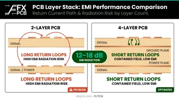
Controlled impedance is a related outcome. Standard controlled-impedance PCB tolerance is ±10%, achievable when trace width, copper thickness, and dielectric spacing are designed and manufactured together — which requires the kind of consistent internal stackup that only multilayer construction provides. SFX PCB holds ±10% impedance tolerance on 4-layer through 8-layer configurations.
When this matters most:
- High-speed digital designs operating above ~200 MHz
- RF and wireless boards where impedance matching is critical
- Medical diagnostic equipment requiring precise analog signal fidelity
- Automotive ADAS systems and telecom infrastructure
EMI failures during FCC or CE testing don't just cost money on the re-test — they require board redesigns. Research from I-Connect007 citing Lifecycle Insights found the average PCB design project requires 2.9 respins, with costs ranging from tens of thousands to millions of dollars. Getting the stackup right before layout begins is the most cost-effective EMI mitigation available.
Advantage 2: Compact Form Factor with Higher Component Density
Board area is a hard constraint in most modern product designs. Wearables, smartphone components, automotive ECUs, and implantable medical devices all have fixed physical envelopes that the PCB must fit within — and those envelopes are getting smaller.
Multilayer boards address this by moving signal routing to internal layers, freeing outer surfaces for component placement. More routing layers mean more traces can be packed into the same footprint, or the same circuit can fit in a significantly smaller board area.
Eliminating the inter-board connectors that would otherwise link multiple single-layer boards also eliminates a common source of assembly failure.
Miniaturization has shifted from a differentiator to a baseline requirement across consumer electronics, medical devices, and automotive systems — and multilayer construction is what makes that density achievable.
Density advantages that matter in practice:
- More routing channels per unit area without violating spacing rules
- Inner layers available for power distribution without consuming outer surface area
- Elimination of external bus connectors between boards reduces assembly complexity
- Smaller enclosures, lower product weight, and in portable devices, longer battery life from reduced board volume
SFX PCB's 8-layer configurations support inner layer trace width and spacing down to 3 mil / 3 mil (0.075mm), enabling the routing density required for dense BGA fanout and high-speed differential pairs in compact designs.
When this matters most:
- Wearable devices and portable medical equipment
- Aerospace avionics where weight budgets are strict
- Smartphones, tablets, and IoT gateways
- Any design where the PCB must fit a constrained enclosure
Advantage 3: Enhanced Durability and Long-Term Structural Reliability
Durability in PCB terms means resistance to the failure modes that matter in field conditions: thermal cycling, mechanical vibration, and long-term environmental exposure. A board that fails in an automotive powertrain module or an industrial controller carries costs that go well beyond the cost of the PCB itself.
Multilayer construction addresses this through two mechanisms. First, the lamination process creates a structurally denser, more rigid board than single or double-layer alternatives — less susceptible to flexion-induced trace cracking in high-vibration environments.
Second, internal copper planes distribute heat more evenly across the board, reducing thermal hotspots that accelerate component and solder joint degradation.
ROHM's testing under JEDEC-based conditions found that 4-layer boards reduced thermal resistance compared to 2-layer boards in identical package configurations. For an HTSOP-J8 package, resistance dropped from approximately 50°C/W to 35°C/W; a TO252-3 package saw a reduction from 25°C/W to 18°C/W.
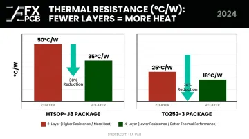
Better thermal management means cooler components, longer solder joint life, and lower field failure rates.
Reliability standards that apply:
- IPC-6012 (Revision F, 2023): Covers qualification and performance for rigid printed boards, including multilayer construction with blind and buried vias
- IPC-6012FA: Automotive addendum addressing printed board reliability in automotive electronic-interconnect environments
- IPC-TM-650: Test methods covering thermal shock, continuity, and vibration for printed boards
When this matters most:
- Industrial automation equipment subject to vibration and thermal cycling
- Automotive powertrain and safety systems operating under-hood
- Aerospace and defense electronics with extended service requirements
- Medical devices where field failure consequences are life-critical
Where Multilayer PCBs Are Used
Medical Devices and Healthcare Equipment
Patient monitors, MRI systems, surgical robotics, and implantable devices all require high component density, precision signal fidelity, and zero-defect reliability. IPC-A-610 Class 2 and Class 3 compliance isn't optional here — it's required by regulators and expected by medical OEMs.
SFX PCB holds ISO 13485 certification and manufactures to IPC-A-610 Class 2/3 standards, supporting applications including:
- ECG monitors and glucose meters
- Surgical robotics and imaging system electronics
- Implantable devices and patient monitoring platforms
Automotive and Aerospace Electronics
ECUs, ADAS systems, flight computers, and navigation platforms rely on multilayer PCBs to manage dense signal routing within strict size and weight envelopes, while surviving extreme thermal and mechanical stress. The automotive addendum IPC-6012FA addresses exactly these conditions, setting the qualification baseline for boards deployed in vehicles and aircraft alike.
Consumer Electronics, Telecommunications, and Industrial Automation
Smartphones, 5G base station equipment, industrial PLCs, and IoT gateways have made multilayer PCBs the default architecture. The routing density these applications demand simply cannot be achieved on two-layer boards at production volumes. Per I-Connect007's reporting, 5G is also accelerating a shift toward higher layer counts and mixed RF-digital designs, with high-speed digital channels now operating at and beyond 112 Gbps per channel.
For industrial customers, SFX PCB's multilayer capabilities cover the layer counts and material specifications needed for thermally demanding environments, including high-Tg laminates rated to 170°C and 180°C.
What Happens When You Choose the Wrong PCB Architecture
Under-specified PCB architecture has a predictable failure sequence.
The issues tend to compound in three stages:
- EMI failures at certification: Routing signal and return paths on the same two-layer board increases loop inductance and radiated emissions. FCC or CE testing fails, triggering a full redesign — new stackup, new layout, new prototypes, and another round of regulatory testing.
- Field failures after launch: Boards that pass initial testing but run near their thermal limits degrade over time. Solder joint fatigue from thermal cycling, trace cracking from vibration, or delamination from marginal lamination quality drives warranty claims and field replacements.
- Workarounds that mask the problem: Larger boards, external shielding, and additional connector assemblies to link multiple single-layer boards each add cost, weight, and failure points — without fixing the underlying architecture.
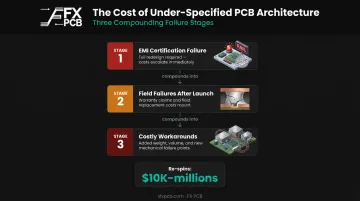
That last point applies equally to stackup selection. ROHM's thermal design guidance puts it plainly: address thermal architecture in the initial development phase, because modifications after the fact are time-consuming and costly. A 4-layer board costs more per unit than a 2-layer board, but that upfront premium is a fraction of a single re-spin, which I-Connect007 reports can range from tens of thousands to millions of dollars.
How to Get the Most Out of Your Multilayer PCB
Plan the Stackup Before Routing
The layer arrangement — signal layers, ground planes, power planes, and their order — determines impedance control, EMI performance, and crosstalk isolation. For a 4-layer board, SFX PCB's recommended stackup is SIG-GND-PWR-SIG, which places every signal trace adjacent to a reference plane and minimizes loop inductance. For 6-layer designs, a dedicated ground plane on Layer 2 and power plane on Layer 4 provides stable references for the internal signal layers.
Establish target impedance values and board thickness before any routing begins. Mid-design stackup changes invalidate completed routing work.
Run DFM Before Fabrication
Multilayer PCBs are substantially more complex to manufacture than single-layer boards. Design issues that are trivial to fix in a CAD file become expensive once boards are in fabrication.
SFX PCB provides a free DFM analysis with every order, performed by engineering staff before production begins. This catches via placement conflicts, trace-to-plane spacing errors, and controlled impedance mismatches before they reach the fab floor.
For customers who haven't finalized their Gerber files, SFX PCB's engineering team can provide stackup recommendations and design guidance before formal submission. Send design files to info@sfxpcb.com and receive a stackup recommendation and quote within 8 hours.
Specify and Verify Electrical Performance
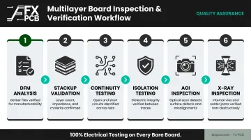
Once DFM clears, verification is the final line of defense. Internal layers cannot be inspected visually after lamination, so SFX PCB runs 100% electrical testing — continuity and isolation — on every bare board before shipping.
For inner-layer registration and buried via integrity, SFX PCB's six-stage inspection process covers:
- Continuity and isolation testing on every bare board
- AOI (Automated Optical Inspection) at critical production stages
- X-ray inspection for inner-layer registration and buried via integrity
Conclusion
Multilayer PCBs deliver compounding engineering advantages that single or double-sided boards can't match: dedicated reference planes for signal integrity, internal routing for miniaturization, and laminated construction for structural reliability. The industries driving modern electronics have standardized on multilayer designs because the performance and reliability stakes are too high for compromise.
That value is only fully realized when design, manufacturing quality, and supplier capability all align. SFX PCB brings all three together with ISO 13485-certified, IPC-A-610 Class 2/3 compliant fabrication and assembly, covering:
- 4-layer prototypes through 68-layer production boards
- Free DFM analysis on every order
- 100% electrical testing on every bare board before it ships
Frequently Asked Questions
What are the advantages of multilayer PCBs?
The three primary advantages are superior signal integrity through dedicated internal ground planes, higher circuit density that enables compact designs, and enhanced structural durability from the laminated construction. These properties translate directly to lower field failure rates, better EMI compliance outcomes, and longer product lifespans.
What are multilayer PCBs used for?
Multilayer PCBs are standard in smartphones, tablets, medical monitors and imaging equipment, automotive ECUs and ADAS systems, aerospace and defense electronics, and 5G telecom infrastructure. They're the default architecture wherever signal performance, routing density, or reliability requirements exceed what two-layer boards can deliver.
How many layers does a multilayer PCB typically have?
Most commercial applications use between 4 and 12 layers. Four-layer boards are the most common entry point for high-speed or EMI-sensitive designs. Layer count is driven by routing density, impedance requirements, and signal isolation needs, not by a fixed standard.
Are multilayer PCBs more expensive than single-layer or double-layer boards?
Per-unit fabrication cost is higher due to additional materials and lamination steps. When total cost of ownership is considered — fewer field failures, eliminated connector assemblies, smaller enclosures — the premium typically pays for itself at production volume.
How do I choose the right number of layers for my PCB design?
Layer count should be driven by routing density, controlled impedance requirements, and EMI constraints. A DFM review early in the design process is the most reliable way to validate a proposed stackup before layout begins.