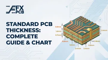
Introduction
PCB thickness is a foundational design parameter that directly shapes mechanical reliability, electrical performance, connector compatibility, and manufacturing feasibility. Every application — from consumer electronics to automotive control units — demands deliberate thickness selection to ensure the board survives its environment and fits its housing.
Many engineers default to 1.6mm — a figure rooted in legacy FR4 fabrication standards and IPC guidelines — without understanding when to deviate or how thickness interacts with layer count, copper weight, and application constraints. The result? Boards that warp during reflow, connectors that don't mate properly, or enclosures that won't close.
This guide covers the full picture: how layer stacks determine final dimensions, application-specific thickness charts, performance trade-offs, and the specification practices that prevent costly redesigns.
Key Takeaways
- Standard PCB thickness is 1.6mm (0.063")—an industry convention chosen for mechanical strength, component compatibility, and manufacturing efficiency
- Final board thickness stacks up from substrate cores, prepreg, copper foils, solder mask, and silkscreen layers
- Thickness requirements vary by application: consumer electronics typically run 0.8–1.0mm, while industrial, automotive, and power boards range from 1.6mm up to 3.2mm
- Non-standard thicknesses add cost and lead time—and can break connector compatibility if not carefully specified
- Always specify nominal thickness plus tolerance in fabrication documentation
What Is Standard PCB Thickness?
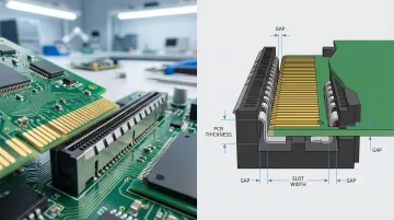
PCB thickness is the total measured distance from the top surface to the bottom surface of a finished board, encompassing all constituent layers—not just the substrate. This is the dimension that appears on fab drawings and determines compatibility with connectors, enclosures, and assembly fixtures.
Why 1.6mm Became the Industry Standard
The 1.6mm (0.063") standard traces back to early electronics manufacturing, when 1/16-inch Bakelite sheets were used as breadboarding substrates. As the industry transitioned to FR-4 fiberglass laminates, legacy tooling, edge-card connectors, and mounting hardware had already standardized around this dimension.
Today, major connector manufacturers like Molex and Samtec continue to design PCI Express and edge-card receptacles specifically for 1.57mm to 1.60mm thick mating boards.
IPC standards do not mandate 1.6mm. IPC-2221A treats board thickness as a design parameter to be optimized for structural, electrical, and thermal needs. The 1.6mm convention persists because it balances board rigidity with weight and fits the vast majority of through-hole lead lengths and connector slot dimensions.
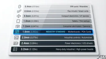
Common PCB Thickness Options
| Thickness (mm) | Thickness (Inches) | Thickness (Mils) | Primary Applications |
|---|---|---|---|
| 0.4mm | 0.016" | 16 mils | Flex-rigid interfaces, SIM cards, ultra-compact wearables |
| 0.6mm | 0.024" | 24 mils | Smartphones, advanced IoT sensors, space-critical modules |
| 0.8mm | 0.031" | 31 mils | Wearables, smart cards, compact consumer electronics |
| 1.0mm | 0.039" | 39 mils | Thin consumer products, laptops, USB modules |
| 1.2mm | 0.047" | 47 mils | General electronics, industrial controls, communication peripherals |
| 1.6mm | 0.063" | 63 mils | Standard motherboards, general-purpose electronics, PCIe cards |
| 2.0mm | 0.079" | 79 mils | Heavy-duty multilayer boards, automotive controllers, server backplanes |
| 2.4mm | 0.094" | 94 mils | High-power applications, heavy industrial machinery |
| 3.2mm | 0.125" | 125 mils | Aerospace systems, extreme high-current power supplies |
Standard vs. Custom Thickness
Most of the thicknesses above fall into two practical categories with very different procurement implications:
- Standard thicknesses are readily stocked by fabricators and processed without lead time penalty
- Custom thicknesses require special material orders and custom lamination press cycles — fabricators report this can increase costs and extend lead times by 50–100% on rush orders
Tolerance Expectations
The 1.6mm figure encompasses a tolerance range. IPC-6012 and industry practice allow ±10% variation for standard boards, meaning a nominal 1.6mm board can range from 1.44mm to 1.76mm. SFX PCB maintains tighter tolerances: ±8% for boards ≥0.8mm and ±10% for boards <0.8mm, ensuring consistent mechanical fit across production runs.
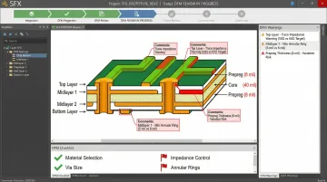
What Determines PCB Thickness: The Layer Stack Explained
Every layer in a PCB contributes measurable thickness. The total board thickness is the sum of these contributions, and changing any parameter—copper weight, core selection, number of prepreg sheets—shifts the final dimension.
Substrate / Core Layers
The substrate core (most commonly FR-4) is the primary structural element. Core thickness is selected from a range of standard values such as 0.005", 0.008", 0.014", 0.021", 0.028", and 0.039". Fabricators stock limited core sizes; using non-stocked cores adds lead time and cost.
Prepreg (pre-impregnated glass/resin material) bonds cores together or bonds cores to external copper foil in multilayer construction. Prepreg thickness is governed by two factors:
- Glass weave style — styles such as 106, 1080, 2116, and 7628 press to different thicknesses: a 106 ply presses to ~0.05mm (2 mils), while a 7628 presses to ~0.18–0.20mm (7–8 mils)
- Resin content (Standard Resin SR, Medium Resin MR, High Resin HR) — affects both prepreg thickness and the dielectric properties that govern impedance control
Copper and Finishing Layers
Copper thickness is specified in ounces per square foot (oz/ft²), where each ounce translates to a fixed physical depth:
| Copper Weight | Nominal Thickness (μm) | Nominal Thickness (mils) |
|---------------|------------------------|--------------------------|
| 0.5 oz | 17.5 μm | 0.69 mils |
| 1 oz | 35 μm | 1.37 mils |
| 2 oz | 70 μm | 2.74 mils |
| 3 oz | 105 μm | 4.11 mils |
Internal layers commonly use 0.5 oz or 1 oz copper, while external layers may go up to 2 oz or higher for power applications. In multilayer boards, each added copper layer compounds the total — a factor that requires careful stack-up planning when boards must fit tight mechanical envelopes.
Solder mask, surface finish, and silkscreen each add smaller but cumulative thickness:
- Solder mask (LPI): 15–25 μm per side
- ENIG finish: 3–6 μm nickel + 0.05 μm gold
- Silkscreen: 20–25 μm
These surface layers add approximately 35–50 μm over bare laminate thickness. In tight enclosures, that margin is the difference between a board that fits and one that requires a costly redesign — which is why understanding the full stack matters before settling on a target thickness.
PCB Thickness by Application and Layer Count
As layer count increases, additional core and prepreg layers are stacked, driving up total board thickness. Maintaining a standard total thickness (e.g., 1.6mm) with more layers requires thinner individual layers, increasing fabrication complexity and cost. Maintaining a standard total thickness (e.g., 1.6mm) with more layers requires thinner individual layers, increasing fabrication complexity and cost. The table below captures practical thickness ranges across the most common layer configurations.
Typical Thickness Ranges by Layer Count
| Layer Count | Minimum Practical | Standard Industry | Maximum Typical |
|---|---|---|---|
| 2-Layer | 0.4mm | 1.6mm | 3.2mm |
| 4-Layer | 0.4mm | 1.6mm | 3.2mm |
| 6-Layer | 0.6mm | 1.6mm | 3.2mm |
| 8-Layer | 0.8mm | 2.0mm | 3.2mm |
| 10-Layer | 1.0mm | 2.0mm | 3.2mm |
| 12-Layer | 1.2mm | 2.4mm | 3.2mm |
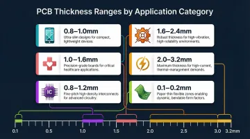
Application-Specific Thickness Guidance
Consumer Electronics & Wearables (0.8–1.0mm):
Space constraints and weight targets push smartphones and wearables to the thinner end of the range — typically 0.8–1.0mm, with some compact designs reaching 0.6mm.
Automotive & Industrial Automation (1.6–2.4mm):
These environments demand mechanical robustness to survive vibration and thermal cycling (-40°C to +125°C). 1.6mm is standard, but 2.0–2.4mm is frequently used for engine control units and industrial PLCs.
Medical Devices (1.0–1.6mm):
Diagnostic equipment typically uses standard 1.6mm boards, while implantables and compact patient-connected sensors rely on thinner 1.0mm boards or ultra-thin flex circuits. SFX PCB holds ISO13485 certification, covering medical-grade dimensional controls and quality assurance for these applications.
Power Electronics & Heavy Copper (2.0–3.2mm):
High-current applications require 2oz to 4oz copper foils. To accommodate the physical volume of this copper and provide adequate thermal mass, these boards typically range from 2.0–3.2mm. SFX PCB manufactures heavy copper PCBs with copper thickness from 2oz to 20oz.
HDI Boards (0.8–1.2mm):
HDI boards rely on laser-drilled microvias, and IPC-2226 sets a maximum aspect ratio of 1:1 (preferably 0.75:1). For a 100μm microvia, dielectric thickness cannot exceed 100μm — which naturally constrains total board thickness to the 0.8–1.2mm range.
Flex PCB Regions (0.1–0.2mm):
To maintain dynamic flexibility without cracking, flex regions of rigid-flex boards (polyimide core + coverlay) are kept exceptionally thin, typically between 0.1mm and 0.2mm. SFX PCB manufactures flex PCBs with maximum thickness ≤0.3mm for mass production.
How PCB Thickness Affects Performance and Manufacturing
Mechanical and Physical Integrity
Greater board thickness increases flexural rigidity and resistance to warpage and vibration-induced stress—critical in automotive, aerospace, and industrial applications where boards are subject to mechanical shock and thermal cycling.
Thinner boards are more susceptible to warping during reflow soldering. IPC-6012 and IPC-A-600 define strict acceptance criteria for board flatness using a metric called "bow and twist":
- For SMT assemblies: Maximum allowable bow and twist is 0.75%
- For through-hole assemblies: Maximum is 1.5%
Exceeding the 0.75% limit on SMT boards frequently leads to coplanarity issues, resulting in open solder joints or cracked components—especially on large BGAs. Asymmetric copper distribution creates CTE mismatches that push boards past these limits.
Best practice: Mirror copper densities, core thicknesses, and prepreg styles across the board's horizontal center axis. This symmetrical approach is the most reliable way to keep bow and twist within spec.
Signal Integrity and Impedance Control
Mechanical stack-up decisions don't just affect stiffness—they directly shape your signal performance. The dielectric thickness between signal layers and reference planes determines controlled impedance trace geometry. According to IPC-2141A, a thinner dielectric layer requires narrower traces to hit the same impedance target (e.g., 50Ω), which reduces routing density.
Key risk: A ±10% tolerance in finished board thickness translates to a roughly equal shift in dielectric height—enough to push impedance out of spec on high-speed layers. Changing overall PCB thickness without revisiting the internal stack-up is a common and costly oversight.
Connector and Assembly Compatibility
Many connectors, card-edge slots, and PCB-to-PCB interconnects are dimensionally specified for a specific board thickness—most commonly 1.6mm. Connector datasheets from Molex and Samtec explicitly specify a mating card thickness of 1.57mm to 1.60mm (±0.16mm tolerance).
Deviating from this standard without validating connector compatibility is a common source of assembly failures. Boards that are too thick can damage connector pins or demand excessive insertion force. Too thin, and you'll see intermittent electrical contact from loose mating.
Specifying PCB Thickness Correctly
Nominal Thickness and Tolerance
For standard digital boards without controlled impedance, simply calling out "1.6mm ±10%" allows the fabricator to use their most cost-effective, standard stock of cores and prepregs.
For high-speed, HDI, or RF boards, engineers must specify the exact core thicknesses, prepreg glass styles (such as 2116, 1080), and copper weights to maintain impedance targets.
Copper Weight Specification
Copper contributes measurably to total board thickness. Specifying heavier external copper (such as 2 oz vs. 1 oz) must be factored into the overall thickness budget—especially in designs with tight enclosure tolerances.
Critical: IPC-6012 Revision F (Clause 3.6.2.14.1) clarifies that internal plated layers follow lower total copper requirements than external layers. If a drawing simply asks for "2 oz copper," fabricators may start with 2 oz foil and plate it up to 3 oz to meet external requirements, increasing costs. Best practice: Explicitly state whether the callout refers to "starting" or "finished" copper weight.
Avoid mismatched copper weights on opposite sides of a core unless electrically necessary — CTE mismatch and warpage risk increase as a result.
Tolerance Stack-Up Risk
If a 1.6mm PCB sits in a housing designed with 0.1mm clearance, a ±10% tolerance means the board could range from 1.44mm to 1.76mm—and the housing design must accommodate this. Recommendation: Validate mechanical fit using worst-case tolerance analysis, not nominal values.
Working with an Experienced Manufacturer
Free DFM (Design for Manufacturability) analysis lets engineers review stack-up and thickness specifications before fabrication begins — catching errors that would otherwise cause costly respins or delayed delivery. SFX PCB includes DFM review on every order, with engineers responding to design questions within 12 hours.
Their DFM process typically flags:
- Insufficient copper-to-edge or feature spacing
- Annular ring violations on drilled pads
- Stack-up feasibility conflicts with target thickness
- Impedance-controlled layer sequencing issues
Frequently Asked Questions
What is the thickness of a classic PCB?
The classic or standard PCB thickness is 1.6mm (approximately 0.063" or 63 mils), which became the industry convention due to its compatibility with common connectors, through-hole components, and manufacturing processes. However, boards can range from under 0.4mm to over 3.2mm depending on application requirements.
What is the standard thickness of a 4 layer PCB?
A 4-layer PCB most commonly targets a finished thickness of 1.6mm (0.063"), achieved through a stack-up of two internal cores and prepreg layers. Thinner options down to 1.0mm or 0.8mm are achievable but require tighter fabrication control, typically for compact electronics.
What is the 3W rule in PCB?
The 3W rule is a trace spacing guideline (not a thickness rule) stating that edge-to-edge spacing between adjacent traces should be at least 3× the trace width to reduce electromagnetic coupling and crosstalk. It applies to PCB layout, not board thickness specification.
Can PCB thickness be customized beyond standard values?
Yes, but custom thicknesses require fabricators to source non-standard materials, often increasing cost and lead time by 50–100%. Only specify custom thickness when mechanically or electrically necessary, and flag the requirement early in the quoting process.
How does copper weight affect total PCB thickness?
Copper weight directly adds to board thickness — 1 oz/ft² copper is approximately 35 μm thick per layer. Boards with multiple heavy-copper layers, for example 2 oz external and 1 oz internal, can add 0.1–0.2mm or more to total thickness, which matters in tight-tolerance designs.
What PCB thickness is best for high-vibration environments?
Thicker boards (1.6mm to 2.4mm or beyond) are recommended for high-vibration environments such as automotive, aerospace, and industrial automation applications. Increased thickness improves flexural rigidity and reduces the risk of solder joint fatigue and board cracking under mechanical shock and thermal cycling stress.