Introduction
Many engineering teams discover quality issues only after boards reach production—or worse, after they've shipped to customers. A single undetected short circuit, misaligned component, or hidden solder void can trigger costly recalls, safety incidents, and reputational damage that far outweigh the investment in proper testing.
PCB testing encompasses the procedures used to verify that a printed circuit board functions correctly, meets design specifications, and is free from defects before integration into larger systems. For safety-critical industries like medical devices, automotive, and aerospace, the consequences of inadequate testing extend beyond cost — they can be life-threatening.
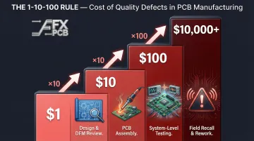
The numbers make the case clearly. According to the 1-10-100 Rule, catching a defect during manufacturing costs $10, but fixing that same defect after deployment escalates to $1,000 or more, with recalls reaching $10,000+ per incident.
That cost gap is exactly why the right testing strategy matters. This guide walks you through every major PCB testing method, explains when to apply each technique, and shows how manufacturers like SFX PCB use layered testing strategies to catch defects at the stage where correction is cheapest and most effective.
TLDR:
- Defect costs multiply 10x at each production stage—catching issues early saves thousands
- No single test catches everything; layered strategies (AOI + X-ray + ICT/Flying Probe + FCT) deliver 95%+ coverage
- AOI inspects visible surfaces in 10-20 seconds but can't see hidden BGA joints—X-ray fills that gap
- ICT suits high-volume stable designs; Flying Probe works for prototypes and frequent revisions
- Functional testing validates real-world performance, catching the 5-10% of defects other methods miss
Why PCB Testing Cannot Be Skipped
Defects originate at multiple manufacturing stages—solder paste printing, component placement, reflow soldering, and final assembly. Without systematic testing, these issues compound into expensive field failures. Research confirms that a defect caught during pre-production costs $1 to fix, but escalates to $10 during assembly, $100 at system-level testing, and $10,000+ if a recall is required.
Real-world recalls show what's at stake when testing gaps go unchecked:
- Philips Respironics settled for $479 million in 2023 after V60 ventilator PCBAs failed to meet power management standards
- Ford recalled 4,632 vehicles when improper solder mask allowed water intrusion, leading to dendritic growth, short circuits, and underhood fires
Safety-Critical Industries and IPC-A-610 Class 3
Those failures aren't outliers—they're the predictable result of skipping rigorous inspection in high-stakes applications. Medical devices, automotive safety systems, and aerospace avionics cannot tolerate field failures. IPC-A-610 Class 3 standards respond to that reality: they mandate zero visible defects, 100% inspection coverage, and strict solder void limits. SFX PCB holds ISO 13485 certification for medical device manufacturing and implements IPC-A-610 Class 2/3 compliance across its quality assurance framework, supporting product acceptance in regulated markets.
Regulatory Compliance Requires Documented Testing
RoHS, REACH, and UL certifications cover chemical safety and component standards—but none of them substitute for electrical functional testing. Global market access requires documented test results, not just certificates. SFX PCB performs 100% electrical testing on every bare board and maintains test documentation to support regulatory compliance and traceability requirements.
The 7 Major PCB Testing Methods Explained
Automated Optical Inspection (AOI)
AOI systems use high-resolution cameras and AI-driven image processing to scan assembled boards against reference designs. The technology detects solder defects, missing components, wrong component orientation, and pad misalignment without physical contact.
Key advantages:
- Inspects boards in 10-20 seconds, ideal for high-volume production
- Achieves 95%+ defect detection rates, reducing escape rates by up to 90%
- Non-destructive and fully automated
Critical limitation: AOI cannot inspect hidden solder joints beneath BGAs or QFNs. It's strictly limited to line-of-sight, making it blind to internal voids, micro-cracks, and connections underneath array packages.
SFX PCB deploys 3D AOI at multiple production stages, catching visible defects immediately after reflow soldering — the point at which 82% of manufacturing faults typically occur.
X-Ray Inspection
Where AOI reaches its limits, X-ray inspection (AXI) takes over. By penetrating the board to image internal solder joints, voids, and connections beneath components, it's the only reliable method for verifying BGA, LGA, and QFN solder quality.
What X-ray detects:
- Solder voids (gas pockets within joints)
- Head-in-Pillow defects (incomplete fusion between solder ball and paste)
- Hidden shorts, bridging, and opens beneath array packages
IPC-7095C void acceptance thresholds:
| Void Location | Class 1 | Class 2 | Class 3 |
|---|---|---|---|
| Within solder ball | Max 25% | Max 25% | Max 20% |
| At package interface | Max 25% | Max 20% | Max 15% |
| At mounting surface | Max 25% | Max 20% | Max 15% |
X-ray is more time-intensive and costly than AOI, making it standard for high-reliability assemblies in aerospace, medical, and automotive sectors. SFX PCB performs in-house X-ray inspection on all BGA assemblies and complex multilayer designs requiring hidden defect verification.
In-Circuit Testing (ICT)
ICT uses a custom "bed-of-nails" fixture: an array of spring-loaded probes that make simultaneous contact with test points across the board. The system measures resistance, capacitance, inductance, and verifies component presence and correct values without powering the full circuit.
Performance metrics:
- Fault coverage: 90-98% for common manufacturing defects
- Test speed: 5-30 seconds per board
- Fixture cost: $5,000-$50,000+ depending on complexity
When ICT makes sense:
- High-volume production (>1,000 units) where fixture cost amortizes quickly
- Stable, mature designs with infrequent revisions
- Boards with accessible test points and adequate spacing
ICT limitations: High component density and fine-pitch components make test pad placement difficult. Moving a single test point by 0.05 inches can render an expensive fixture obsolete.
Flying Probe Testing
For designs where ICT fixture costs aren't justified, flying probe testing (FICT) is the practical alternative. Four to eight software-controlled probes navigate to programmed test points, covering the same electrical checks (opens, shorts, component values) without any fixture investment.
Key differentiators:
- Zero fixture cost (programming runs $500-$2,000)
- Can probe micro-pads down to 80 microns (ideal for HDI boards)
- Setup takes hours instead of weeks
Trade-off: Test cycles take 1-15 minutes per board versus ICT's 5-30 seconds.
Ideal applications:
- Prototypes and low-volume runs (<1,000 units)
- Frequently revised designs where fixture modifications would be costly
- High-density interconnect boards where ICT pogo pins cannot fit
Functional Circuit Testing (FCT)
FCT powers the assembled board and simulates real-world operating conditions by feeding input signals and measuring outputs to confirm the board performs its intended function.
What FCT validates:
- Power supply behavior under load
- Digital and analog I/O signal integrity
- Communication port functionality
- Sensor response and circuit logic
Coverage gap FCT fills: While AOI and ICT catch 90% of structural defects, they miss parametric, timing, and firmware issues. FCT catches the remaining 5-10% of defects, pushing total coverage above 95%.
FCT requires custom test fixtures designed for each specific product, making it a later-stage test applied after other methods have screened for basic assembly defects. SFX PCB develops custom test fixtures in-house, with simple fixtures completed in days and complex ones requiring several weeks depending on project specifications.
Burn-In Testing
Burn-in operates PCBs continuously under elevated temperature, voltage, or load for a set period to force early-life (infant mortality) failures to surface before shipping.
Reliability model: The JEDEC bathtub curve shows failure rates peak immediately after manufacturing, then drop to a low constant rate during normal operation. Burn-in artificially accelerates this early-life phase, surfacing latent defects during production rather than after delivery.
Industry mandates:
- Aerospace: AS9100 environments integrate Environmental Stress Screening (ESS)
- Medical devices: ISO 13485 facilities use burn-in for life-support equipment
- Military: MIL-STD-883 Method 1015 governs burn-in parameters
Burn-in is not universal — it consumes board life, adds time and cost, and isn't needed for consumer electronics where field failure tolerance is higher.
Visual Inspection
Despite advances in automated inspection, manual visual inspection still plays a practical role. Trained technicians examine solder joints, component placement, polarity, and board cleanliness using eyes or low-magnification tools.
Strengths:
- Fast and low-cost first-pass screen
- Detects obvious physical damage, contamination, and gross defects
Limitations:
- Subject to human subjectivity and fatigue
- Cannot detect hidden or microscopic defects
- Inconsistent compared to automated methods
SFX PCB integrates visual inspection checkpoints at incoming goods verification, post-soldering, and final quality control stages — used alongside automated methods rather than in place of them.
How to Choose the Right PCB Testing Method
No single method catches all defect types. The right strategy layers complementary techniques based on board complexity, production volume, application criticality, and budget.
Production Volume Drives Method Selection
| Production Profile | Primary Electrical Test | Inspection Layer |
|---|---|---|
| Prototypes / Low Volume (<1,000) | Flying Probe | AOI (100%) + AXI (if BGAs present) |
| High Volume (>1,000) | ICT / Bed-of-Nails | AOI (100%) + AXI (sample or 100%) |
| High Density / Fine Pitch (HDI) | Flying Probe or Boundary Scan | AOI + AXI (mandatory) |
| Class 3 / Mission Critical | ICT + FCT + Burn-In | AOI (100%) + AXI (100%) |
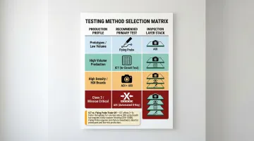
Volume-based decision: ICT provides fast throughput (5-30 seconds per board) once the fixture is built, making it cost-effective for runs exceeding 1,000-10,000 units. Flying probe eliminates fixture cost but takes 1-15 minutes per board—ideal for prototypes and small batches where ICT investment can't be justified.
Application Criticality Determines Coverage Depth
The stakes of a board failure determine how many test layers you need. Two common stacks:
- Consumer electronics: AOI + flying probe + FCT covers most defect categories at reasonable cost
- Medical, automotive, and aerospace: X-ray + ICT or flying probe + FCT + burn-in to meet Class 3 reliability standards
Manufacturers like SFX PCB run AOI, X-ray, and functional testing in-house, which removes the lead-time penalty of outsourcing each layer to separate vendors.
Functional Testing Should Always Be Included
Functional testing validates that the board performs its intended real-world function—not just that components are present and connected. Solder bridges, marginal joints, and parametric drift can all pass structural inspection yet cause field failures. FCT is the stage where those escapes surface.
PCB Testing at Every Stage of Manufacturing
Pre-Production: DFM Analysis and Design Rule Checks
Design for Manufacturability (DFM) analysis identifies potential issues in the PCB layout before fabrication begins. This prevents downstream defects by ensuring trace widths, clearances, annular rings, and test point access align with manufacturing capabilities.
SFX PCB provides free DFM analysis for every order, with engineers reviewing Gerber files within 12 hours to flag insufficient spacing, annular ring issues, and layout problems that could compromise manufacturability or testability.
In-Process Testing During Fabrication and Assembly
Bare board electrical testing verifies continuity (no opens) and isolation (no shorts) before components are assembled. IPC-9252B sets the parameters for both direct resistive testing and indirect adjacency testing — the two methods most fabricators use to meet electrical test requirements.
Assembly checkpoints:
- Solder Paste Inspection (SPI) after paste printing
- AOI after component placement and after reflow soldering
- X-ray inspection for BGA assemblies
Catching defects during fabrication or assembly keeps correction costs low. Each stage that passes without detection makes rework significantly more expensive — and more disruptive to your schedule.
Post-Assembly Final Testing
Once assembly is complete, the final testing stage acts as the last gate before shipment. This phase typically includes:
- Functional testing (FCT) to verify the board performs to specification under real operating conditions
- Burn-in testing for high-reliability products, stressing the board to surface early-life failures
- IPC-A-610 quality inspection to confirm workmanship meets Class 2 or Class 3 standards
SFX PCB implements final quality control inspection before packing and delivery, ensuring every board passes electrical, functional, and visual checks before leaving the facility.
PCB Testing Best Practices
Design Test Coverage at the Layout Stage
Test point access should be built into the PCB layout—not added as an afterthought. IPC-2221A requires test lands for ICT probing to be at least 0.9 mm in diameter and placed 0.6–5 mm away from tall components to allow fixture clearance.
For flying probe testing, test pads should be a minimum of 10 mils (0.254 mm), though 20 mils (0.5 mm) is recommended, with spacing of at least 16 mils (0.4 mm).
Document All Test Procedures and Results
Traceability is essential for regulatory compliance, failure analysis, and continuous improvement. Two key standards define documentation requirements:
- ISO 9001:2015 (Clause 7.5): Requires strict control of documented information, ensuring test records and inspection logs are maintained and protected.
- ISO 13485:2016 (Clause 7.5.1/7.5.8): Mandates that medical device manufacturers maintain a Device History Record (DHR) for each batch, with full traceability of component lots, AOI/AXI inspection records, and FCT acceptance data tied to specific serial numbers.
SFX PCB holds ISO 9001, ISO 14001, and ISO 13485 certifications, requiring documented test records at every production stage.
Qualify Manufacturing Partners by Testing Capabilities
Look for IPC-A-610 Class 2 or Class 3 compliance, ISO certifications, and demonstrated capability with both automated (AOI, X-ray) and electrical testing methods. Quality needs to be embedded in the process, not applied as a final checkpoint.
SFX PCB's certifications include:
- ISO 9001 (quality management)
- ISO 14001 (environmental management)
- ISO 13485 (medical device manufacturing)
- IPC-A-610 Class 2/3 compliance
- RoHS, REACH, and UL compliance
With over 15 years serving medical, automotive, aerospace, and industrial customers, SFX PCB integrates testing at every manufacturing stage. That includes free DFM analysis, 100% electrical testing, AOI, X-ray inspection, and functional testing with custom-developed fixtures.
Frequently Asked Questions
What does PCB stand for?
PCB stands for Printed Circuit Board—a flat board made of insulating material with conductive copper traces that mechanically support and electrically connect electronic components. PCBs form the foundation of virtually all modern electronic devices.
What are the 7 types of PCB testing methods?
The seven main methods are Visual Inspection, Automated Optical Inspection (AOI), X-Ray Inspection, In-Circuit Testing (ICT), Flying Probe Testing, Functional Circuit Testing (FCT), and Burn-In Testing. Most manufacturers combine several of these for comprehensive coverage.
What is reliability testing of PCB?
Reliability testing evaluates a PCB's ability to perform consistently over time under real-world stress conditions — heat, humidity, vibration, and thermal cycling. Methods like burn-in and environmental stress screening are standard practice for aerospace, medical, and military applications.
What is the 3W rule in PCB?
The 3W rule is a PCB design guideline stating that edge-to-edge spacing between two traces should be at least three times the trace width to minimize electromagnetic coupling and signal interference. It's a design rule, not a testing method.
What is the difference between ICT and functional testing?
ICT checks individual component values and connectivity using a fixed-probe fixture without fully powering the board. Functional testing powers the board and verifies that it performs its intended real-world function. They are complementary—ICT catches assembly defects, while FCT validates actual performance.
At what stage of production should PCB testing be performed?
Testing should occur at every stage of production:
- Pre-production: DFM checks before fabrication begins
- During fabrication/assembly: AOI and bare board electrical testing
- Post-assembly: Functional testing and burn-in
Catching defects early at each stage keeps correction costs low and prevents failures downstream.