Introduction
A single undetected fault—a solder bridge, an open trace, a misaligned component—can trigger device failure, safety hazards, or costly product recalls. Poor quality in electronics manufacturing can consume 10-20% of a company's revenue in severe cases.
The 1-10-100-10,000 rule makes the financial stakes concrete: catching a defect at raw materials inspection costs roughly $1; at the deviation stage, $10; during corrective action, $100; at a customer complaint, $1,000; and a product recall costs $10,000 or more. The earlier you catch it, the less it costs.
This guide covers the essential tools, three key testing methods with step-by-step procedures, how to read results accurately, and the most common mistakes engineers and technicians make when testing PCBs. Whether you're troubleshooting a prototype or validating production boards, understanding how to test circuit boards properly prevents field failures and protects your reputation.
Key Takeaways
- Testing requires the right tools (multimeter, magnification, probes) and a sequenced approach—start with visual checks before applying power
- Three core methods cover most needs: manual visual/multimeter testing, in-circuit/flying probe electrical testing, and automated testing (AOI, X-Ray, FCT)
- Results fall into three categories: acceptable, minor deviation requiring monitoring, and out-of-spec requiring rework
- Common errors include probing wrong test points, skipping power-off precautions, and misreading continuity without cross-referencing schematics
- AOI, X-Ray, and functional testing (FCT) should be standard in any PCBA manufacturing workflow, particularly for high-reliability applications
What You Need to Test a Circuit Board
Effective PCB testing starts before any probe touches the board. Having the right tools and establishing the correct board state—powered off, electrostatically discharged, properly illuminated—determines whether your results will be reliable or misleading.
Tools and Equipment Required
Essential bench-level testing tools include:
- Digital multimeter with continuity, resistance, and DC voltage modes (industry-standard 6½ digit bench DMMs provide DC voltage ranges from 100 mV to 1,000 V and resistance ranges from 100 Ω to 1,000 MΩ)
- Magnifying glass or digital microscope (10x–40x magnification)—IPC-OI-645 specifies 4X-7X for SMT solder joints and 7X-10X for fine-pitch components
- Anti-static wrist strap and ESD mat—ANSI/ESD S20.20 compliance is mandatory, with wrist straps measuring between 0.8 × 10⁶ to 1.2 × 10⁶ ohms
- Needle-tip test probes for precise contact with test points
- Board schematic/reference designator list for cross-referencing test results
- Controlled power supply for functional checks
Professional facilities add specialized equipment: bed-of-nails ICT fixtures, flying probe machines, AOI cameras, X-ray systems, and functional test jigs. The level of tooling scales with production volume and fault coverage requirements.
Preconditions and Setup
Before running any test, confirm these conditions are met:
- Power off first: Start with the board fully powered down and discharged unless the method (voltage rail measurement, FCT) explicitly requires live power. Always disconnect circuit power and discharge all high-voltage capacitors before continuity testing to avoid damaging the meter or components.
- Prepare the surface: Place the board on an ESD-safe, level, well-lit surface. Clean flux residue before visual or automated optical inspection—contamination causes false-positive defect readings and degrades probe contact resistance.
Methods to Test a Circuit Board
No single method catches every fault. Choose based on what stage the board is at (bare PCB, assembled, prototype vs. production), what faults are suspected, and what equipment is available. Layering methods delivers the highest fault coverage.
Method 1: Visual Inspection and Multimeter Testing
The first-pass method for any circuit board. Visual inspection identifies physical defects (solder bridges, tombstoned components, cold joints, burn marks, missing parts), while multimeter testing verifies electrical continuity of traces and detects short circuits or open circuits without requiring operational power.
Tools Needed:
- Digital multimeter set to continuity mode (audible beep)
- Magnifying glass or digital microscope
- PCB schematic or layout reference
- ESD protection
Step-by-Step:
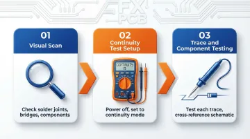
Visual scan: Under magnification, systematically examine solder joints for cold/dull appearance, bridges between pads, missing or misaligned components, burnt or discolored areas, and cracked traces. Mark any anomalies against the reference layout. IPC-A-610 standards classify cold solder joints with rough surfaces and abnormal wetting angles as defects across all classes.
Continuity test setup: Power off the board completely. Insert the red probe into the "V" socket and black into "COM" on the multimeter. Select continuity mode and verify the tester by touching the probes together—you should hear an audible beep confirming the function is active (most multimeters beep at 40 Ω or less resistance).
Trace and component testing: Place one probe at each end of a suspicious trace or across component terminals. A continuous beep confirms connection (no open); silence on a trace that should conduct, or a beep across two pads that should be isolated, indicates a fault. Always cross-reference against the schematic before concluding—some traces are deliberately connected and some components have near-zero resistance by design.
Pros & Cons:
Pros:
- Zero-cost entry point requiring no specialized equipment
- Fast setup — valid as the mandatory first step in any testing sequence
Cons:
- Manual inspection detects only 85-90% of defects and processes just 500-800 components per hour due to fatigue
- Cannot detect hidden solder defects under BGA packages, incorrect component values, or performance/timing faults
Method 2: In-Circuit Testing (ICT) and Flying Probe Testing
Both methods make direct electrical contact with test points on the assembled PCB to measure component values (resistance, capacitance, inductance) and verify circuit connectivity—detecting shorts, opens, wrong or reversed components, and incorrect values without requiring the board to perform its intended function.
Tools Needed:
- ICT uses a custom "bed of nails" fixture (spring-loaded pins contacting all test points simultaneously)
- Flying probe uses a programmable machine with movable probe arms that contact individual test points sequentially
- Both connect to measurement hardware and test software
Step-by-Step:
Test program/fixture setup: For ICT, load the board-specific test fixture and the net-list-derived test program. For flying probe, import the board's CAD data and define the probe sequence. Both require reference to the schematic to define expected values and pass/fail thresholds.
Board loading and contact verification: Place the board onto the fixture (ICT) or into the flying probe machine. Confirm all probes make reliable contact with test points—miscontact is the leading cause of false failures. CAD files with <0.05 mm Gerber drift can cause misaligned probes, leading to 20% false opens.
Run the test and log results: Execute the test sequence. The system automatically measures each parameter against defined limits and flags deviations. Review the fault log, isolating shorts (lower-than-expected resistance between isolated nodes) from opens (no continuity on connected nets) for targeted rework.
Pros & Cons:
ICT pros:
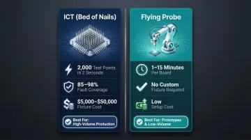
- Completes 2,000 test point contacts in 2 seconds with 85-98% fault coverage
- Best suited for high-volume production runs
ICT cons:
- Fixtures cost $5,000–$50,000+ per design with 4-6 week lead times — cost-prohibitive for prototypes
Flying probe pros:
- Fixture-free setup, making it practical for prototypes and low-to-medium runs
Flying probe cons:
- Up to 60x slower than ICT: 1-15 minutes per board versus 5-30 seconds for ICT
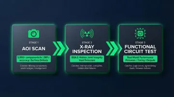
Method 3: Automated Optical Inspection (AOI), X-Ray Inspection, and Functional Circuit Testing (FCT)
Three complementary automated methods used in professional manufacturing. AOI scans the board surface using cameras and algorithms to catch visual defects at speed; X-ray inspection reveals hidden solder quality under BGAs and in vias invisible to the eye; FCT applies actual operating power and signals to confirm the board performs its intended function end-to-end.
Tools Needed:
- AOI machine with high-resolution cameras and defect-classification software
- X-ray inspection system (2D or 3D CT)
- Custom FCT jig with power supply, signal generators, and measurement instruments matched to the board's functional specification
- Test software to automate pass/fail evaluation
Step-by-Step:
AOI scan: Feed the assembled board through the AOI system. The machine compares captured images against the golden reference or CAD data, flagging misaligned components, solder bridges, missing parts, and insufficient solder. Automated optical inspection examines 5,000+ components per hour with 98%+ accuracy, compared to 500-800 components per hour for manual inspection. Modern AI-driven 3D AOI systems eliminate 50-100% of false calls, reducing review times by up to 90%.
X-ray inspection for hidden joints: For boards with BGAs, QFNs, or other bottom-terminated packages, use X-ray to image solder ball integrity beneath the package. Because BGA joints are sandwiched between the component and the PCB, visual inspection is useless—X-ray is mandatory. Look for voids exceeding the IPC-A-610 acceptance criteria; for most applications, BGA voiding should be kept below 25% of the solder joint area.
Functional Circuit Test: Connect the board to the FCT jig, apply rated power, and execute the test sequence—stimulating inputs and measuring outputs against specification. A pass confirms the board performs as designed under realistic conditions. FCT detects incorrect firmware, timing issues, output voltage errors, and communication protocol faults that ICT cannot catch.
Pros & Cons:
Pros:
- Highest combined fault coverage available — catches visible defects, hidden solder failures, and performance issues in a single pipeline
- AOI and X-ray run at production speed with minimal operator intervention
Cons:
- All three require upfront equipment investment and test program development
- FCT identifies that a board has failed but doesn't always isolate the defective component — additional debugging is often needed
When sourcing assemblies externally, confirm that AOI, X-ray, and FCT are included in the manufacturer's quality process, not offered as optional add-ons. SFX PCB runs all three as part of its standard PCBA workflow, with 100% electrical testing on every bare board and IPC-A-610 Class 2/3 compliance across assemblies.
How to Interpret PCB Test Results
Collecting test data is only half the job. Misinterpreting results causes good boards to be scrapped (false failures) or faulty boards to pass (false escapes). Understanding the three outcome categories and the right action for each prevents both.
Normal/Acceptable
A pass result means:
- Continuity is confirmed on all connected nets
- No continuity exists between isolated nodes
- Component values fall within the ±tolerance specified on the BOM
- AOI shows no flagged anomalies
- FCT outputs match specification under full operating load
Document the pass record and move to the next stage.
Minor Issues / Marginal Readings
Readings that fall within tolerance but near the limit—such as a resistor measuring at the edge of its tolerance band or a solder joint flagged by AOI but visually acceptable under magnification—warrant closer inspection and re-test rather than an immediate pass or reject.
IPC-A-610 defines "Process Indicators" as conditions that deviate from full acceptability but do not impact form, fit, or function. Single instances do not require rework or scrapping.
For borderline visual calls, perform a referee inspection using 10X magnification to verify any product rejected at the standard inspection magnification.
Out-of-Spec / Fault Confirmed
Solder bridge: A beep between nodes that should be isolated signals a solder bridge or PCB trace short. Locate it visually under magnification and reflow or remove excess solder.
Open circuit: Silence on a trace that should conduct indicates an open. Inspect for cracked traces, lifted pads, or cold joints and re-solder or re-route.
Wrong component value: A component measuring outside its rated value indicates wrong or damaged part—replace from BOM-verified stock.
FCT failure with ICT pass: This suggests a design or firmware issue rather than a manufacturing defect—escalate to the design team.
Always cross-reference test output against the board's schematic and layout before classifying a result as a defect. A multimeter beep without schematic verification may flag an intentional connection as a fault.
Common Mistakes When Testing a Circuit Board
A few recurring errors account for the majority of misdiagnosed boards. Catching them early saves time, components, and rework costs.
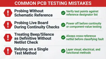
- Probing without a schematic open for reference leads to mistaking adjacent pads for the intended test point — especially on fine-pitch or dense boards. Always verify test points against the reference designator list before touching anything.
- Applying probes to a live board during continuity or component-value checks risks ESD damage and false readings from parallel circuit paths. Power off first unless you're explicitly measuring voltage.
- Treating a continuity beep as proof of a short — or silence as proof of an open — without checking the netlist is one of the most common sources of false failures. Some traces are deliberately connected; some components have near-zero resistance by design.
- Relying on a single test method leaves real faults undetected. Error rates of 20–30% are frequently cited in inspection literature, even under 100% inspection coverage. Visual checks miss hidden solder defects, multimeters miss performance faults, and FCT alone won't locate which component failed. Combining methods isn't optional for reliable fault coverage.
Safety and Best Practices for PCB Testing
ESD Protection
Always wear an anti-static wrist strap connected to a grounded ESD mat when handling bare boards or populated assemblies. According to industry studies, up to 90% of ESD-related failures stem from latent damage rather than immediate catastrophic events — components pass manufacturing tests but fail unpredictably in the field.
Isolation Before Testing
Confirm the board is fully de-energized and all capacitors are discharged before touching or probing components. Use a discharge resistor on high-capacitance power rails. Only perform powered testing for voltage measurements and functional checks, always using insulated probes.
Cleanliness
Remove flux residue with an appropriate solvent before AOI or visual inspection. Residue mimics solder bridges under optical systems and triggers false defect calls. IPC-A-610 outlines strict cleanliness requirements, noting that flux residues from no-clean processes must meet specific appearance criteria to prevent electrochemical migration.
Documentation Discipline
Record every test result, tool calibration date, and board serial number. Without traceable records, root cause analysis becomes impossible when field failures occur.
Maintain a consistent ESD equipment check schedule:
- Test wrist straps daily — wear degrades the grounding connection over time
- Inspect worksurfaces quarterly for wear or contamination that could compromise grounding
- Log all equipment checks alongside board test records for full traceability
With safety protocols in place, you're ready to move into the testing methods themselves.
Conclusion
Effective PCB testing works in layers. Visual inspection catches surface defects early, electrical measurement confirms continuity and isolation, and functional testing validates real-world behavior. Each method targets a different class of defect — skip one, and you leave gaps that can reach the field.
Accurate test interpretation—cross-referenced against the schematic and IPC acceptance standards—is what separates a reliable quality gate from a false sense of assurance. Defining pass/fail criteria before testing begins is just as important as the tests themselves — without clear thresholds, even a comprehensive process produces ambiguous results.
For teams that want testing embedded in manufacturing from the start, SFX PCB applies 100% electrical testing on every bare board, combined with AOI, X-ray inspection, and IPC-A-610 Class 2/3 assembly standards — so defects are identified at the source, not discovered after delivery.
Frequently Asked Questions
How can you tell if a circuit board is bad?
Visible burn marks, bulging or cracked components, and the smell of burnt electronics are immediate red flags. A multimeter continuity test revealing shorts between isolated nets or open circuits on connected traces confirms electrical faults. Boards that pass visual and continuity checks but fail functional testing indicate a performance-level defect.
What tools do I need to test a circuit board at home?
A digital multimeter (with continuity and DC voltage modes) and a magnifying glass are the minimum for basic testing. An ESD wrist strap and an ESD mat are essential to avoid damaging components. A schematic or layout reference is non-negotiable for interpreting any test result accurately.
What is the difference between ICT and flying probe testing?
ICT uses a fixed "bed of nails" fixture that contacts all test points simultaneously, making it fast and well-suited to high-volume production. Flying probe uses movable arms to test points sequentially with no custom fixture required — flexible and cost-effective for prototypes and low-volume runs, though significantly slower.
Can I test a circuit board without powering it on?
Yes, visual inspection, continuity testing, and in-circuit/flying probe methods are all performed without applying operating power. Powering the board is only required for voltage rail measurements and functional testing; when you do, use insulated probes and follow appropriate safety precautions.
What does a continuity test on a PCB actually verify?
A continuity test checks whether an electrical path exists between two points — a beep confirms the path is intact (no open circuit), while silence on a trace that should conduct indicates a broken connection. It also detects unwanted shorts by revealing continuity between nodes that the schematic shows should be electrically isolated.
When should I use automated PCB testing over manual methods?
Automated testing (AOI, ICT, FCT) becomes necessary in three situations:
- Production volume makes manual inspection impractical
- Boards contain hidden joints (BGAs, QFNs) unreachable by visual or probe methods
- The application demands high reliability (medical, automotive, aerospace) where human-inspection error rates are not acceptable