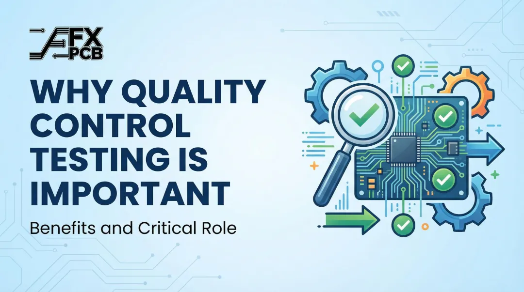
Introduction
A PCB defect caught during manufacturing costs a fraction of what it costs after deployment. In high-stakes industries, the consequences go beyond rework costs:
- FDA Class I recalls for ventilators with faulty power management PCBAs
- Ford recalling thousands of vehicles due to battery junction box failures causing underhood fires
- Cummins/Daimler trucks recalled because defective solder joints caused engine stalls
These aren't hypothetical risks. They're real-world failures that illustrate a fundamental truth: PCB quality validation is a business-critical concern, not just a technical checkbox. The 1-10-100 Rule of quality economics, originally developed by quality management researchers, puts hard numbers to this: a defect costs $1 to fix during design, $10 during assembly, and $100 or more once it reaches the field. Each stage multiplies the cost by an order of magnitude.
PCB quality encompasses two critical dimensions: conformance to design specifications AND adherence to industry standards (IPC, ISO, RoHS). This guide covers both the testing methods that validate quality and the standards that govern them, providing a complete roadmap from DFM review through final inspection.
Key Takeaways
- PCB quality validation spans multiple testing stages: visual inspection, electrical testing, functional verification, and environmental stress testing
- Key methods—AOI, X-Ray, ICT, Flying Probe, FCT, and Burn-In Testing—each target different board types, volumes, and defect profiles
- Industry standards such as IPC-A-610, IPC-6012, and ISO 9001 define the pass/fail benchmarks manufacturers must meet
- Embed testing across the full production process—from DFM review pre-manufacturing through final inspection before shipment
- Certified quality processes (IPC-A-610 Class 2/3, ISO 13485) are the clearest signal a manufacturer will catch defects before they reach the field
What Is PCB Quality — and What Does Poor Quality Actually Cost?
A board can look perfect and still fail in the field. PCB quality is the degree to which a board meets its functional, structural, and compliance specifications — covering dimensional accuracy, soldering integrity, electrical performance, and material compliance with standards like RoHS and REACH.
The Root Causes of PCB Quality Failures
Most PCB quality failures fall into three categories, each requiring different test methods to detect:
- Design issues caught through DFM (Design for Manufacturability) review—insufficient trace spacing, undersized annular rings, improper solder mask clearances
- Process defects during manufacturing—soldering problems, component misplacement, open/short circuits
- Material non-conformance—failure to meet RoHS, REACH, or other regulatory requirements
According to iNEMI research on SMT assembly, 60% to 70% of all SMT assembly defects originate from a single step: solder paste printing. Insufficient solder volume, clogged stencil apertures, and poor paste rheology all feed directly into downstream failures — tombstoning, solder bridges, and cold joints.
Knowing where defects originate is half the equation. The other half is understanding what it costs when they go undetected.
The Economics of Late Detection
Electronics manufacturing follows the "1-10-100 Rule," a Cost of Quality (COQ) model defined by the American Society for Quality: catching a defect earlier is always cheaper than catching it later.
Cost escalation across the product lifecycle:
- $1 at design stage — DFM review catches issues before manufacturing begins
- $10 during assembly — Internal failure costs like rework and scrap
- $100+ in the field — External failure costs including warranty claims, recalls, and reputation damage
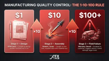
For medical devices or automotive applications, that field-failure multiplier climbs far beyond 100x once regulatory penalties and liability exposure enter the picture.
Key PCB Quality Standards You Need to Know
IPC-A-610J: The Global Benchmark for Assembly Quality
IPC-A-610, "Acceptability of Electronic Assemblies," is the most widely used electronics assembly acceptance standard globally. The current revision, IPC-A-610J, was released in March 2024 and defines visual quality acceptability requirements across three distinct classes:
| IPC Class | Classification | Reliability Expectation | Typical Applications |
|---|---|---|---|
| Class 1 | General Electronic Products | Functionality is primary; cosmetic imperfections acceptable if operation unaffected | Consumer electronics, toys, disposable products |
| Class 2 | Dedicated Service Electronics | Continued performance and extended life required; uninterrupted service desired but not critical | Telecommunications, industrial controls, laptops |
| Class 3 | High Performance Electronics | Mission-critical performance; equipment downtime cannot be tolerated; harsh environments | Aerospace, military, medical life-support, automotive safety |
Critical distinction: A defect for Class 1 automatically implies a defect for Classes 2 and 3, but the reverse isn't true. OEMs must explicitly specify the required IPC Class in procurement contracts to ensure manufacturers align inspection tolerances with product reliability needs.
IPC-6012F and IPC-2221C: Governing Bare Board Fabrication and Design
While IPC-A-610 governs assembled boards, bare board fabrication and design follow separate foundational standards:
- IPC-6012F (Released September 2023): "Qualification and Performance Specification for Rigid Printed Boards" establishes benchmarks for bare board manufacturing, addressing final finish, surface plating, conductor spacing, hole registration, and microvia reliability
- IPC-2221C (Released December 2023): "Generic Standard on Printed Board Design" sets baseline requirements for materials, conductor spacing, electrical clearance, and manufacturability across all PCB design documents
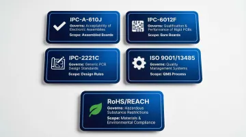
ISO 9001 & ISO 13485: Process-Level QMS vs. Product Certification
ISO certifications govern how a manufacturer operates—not whether a specific board passes inspection. ISO 9001:2015 establishes Quality Management System (QMS) requirements applicable across industries, while ISO 13485:2016 applies those principles specifically to medical device manufacturing.
Both standards provide frameworks for consistent design, production, and risk management. Neither certifies the physical reliability of an individual circuit board—that's what IPC-A-610 and electrical testing are for.
RoHS & REACH: Material-Level Compliance Requirements
Environmental compliance requires strict material-level documentation:
- RoHS Directive (2011/65/EU): Restricts ten hazardous substances — including lead, cadmium, and hexavalent chromium — in electrical and electronic equipment. Compliance requires an EU Declaration of Conformity.
- REACH Regulation: Shifts chemical risk management responsibility to manufacturers and suppliers. Under Article 33, any article containing Substances of Very High Concern (SVHC) above 0.1% concentration requires safety communication down the supply chain.
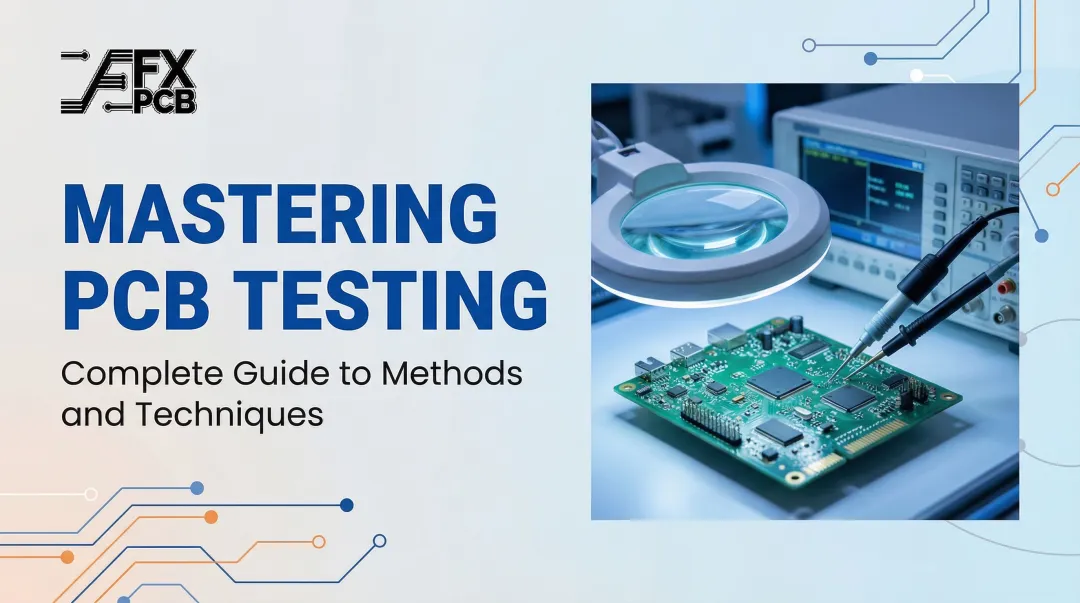
PCB Testing Methods: From Visual to Functional
Automated Optical Inspection (AOI)
AOI uses high-resolution cameras and image-processing software to scan completed PCBs against a reference model. It's typically performed after solder paste application (pre-reflow) and after reflow soldering (post-reflow) to catch surface-level defects.
Common defects detected:
- Component misalignment and incorrect orientation
- Missing or incorrect components
- Solder bridges and insufficient solder
- Polarity errors and tombstoning
AOI is limited to line-of-sight inspection and cannot inspect hidden joints beneath BGA packages—where X-Ray inspection takes over.
X-Ray Inspection (AXI)
Automated X-Ray Inspection uses X-ray penetration to image internal board structures, making it essential for inspecting Ball Grid Arrays (BGAs), QFN, and CSP packages where solder joints are hidden beneath components.
Common defects detected:
- Solder voids and BGA ball misalignment
- Internal layer delamination
- Insufficient solder fill in vias
- Head-in-pillow defects
IPC J-STD-001 mandates that BGA solder voids must not exceed 25% of the joint area.
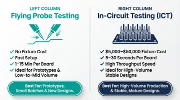
In-Circuit Testing (ICT)
ICT uses a custom "bed of nails" fixture to contact all accessible test points simultaneously, measuring resistance, capacitance, inductance, and verifying component values. Best suited for high-volume production runs of the same board design.
Common defects detected:
- Incorrect component values
- Shorts, opens, and missing components
- Solder joint defects
ICT fixtures cost $5,000 to $50,000+ but test boards in 5-30 seconds—making ICT cost-effective only for high-volume, stable designs.
Flying Probe Testing
Flying probe testing is a fixtureless electrical test where software-guided probes move dynamically across the board to test nodes. It covers the same electrical checks as ICT without needing custom tooling.
Compared to ICT, the trade-offs are straightforward:
- No upfront fixture cost or NRE investment
- Faster setup with no custom tooling to design or manufacture
- Slower test cycle: 1-15 minutes per board versus 5-30 seconds for ICT
Functional Circuit Testing (FCT)
FCT powers up the assembled PCB and simulates its actual operating environment using custom test fixtures and software to verify the board performs its intended functions. This validates full system-level performance, not just individual component values.
While ICT and Flying Probe verify that components are placed correctly with right values, FCT verifies that the board actually works under real-world loads. FCT is typically the final test before shipment, and its complexity scales with board design.
Burn-In Testing
Burn-in testing subjects completed PCBs to extended operation at elevated temperatures and electrical stress to accelerate early-life failures—commonly called infant mortality failures. It's most common in aerospace, military, and medical device manufacturing where field failures carry serious consequences.
The bathtub curve failure model (MIL-HDBK-217) explains why: components face peak failure rates early in their lifespan due to manufacturing anomalies. Burn-in stress eliminates those weak units before they reach the field.
The process is expensive and time-consuming, so it's reserved for applications where a field failure is simply not an option.
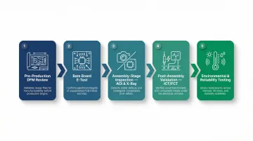
The PCB Quality Validation Process: Stage by Stage
Effective PCB quality validation runs through every phase of manufacturing, not just a final inspection at the end of the line.
Stage 1: Pre-Production DFM Review
Design for Manufacturability (DFM) review analyzes design files to identify manufacturability issues before a single board is made. DFM checks evaluate real-world fabrication capabilities, flagging issues like insufficient trace spacing, undersized annular rings, and thermal design flaws.
Cost benefit: Problems caught at this stage cost the least to fix and directly reduce downstream defect rates.
Stage 2: Bare Board Electrical Testing (E-Test)
IPC-9252B defines standards for electrical testing of unpopulated printed boards. This includes 100% continuity and isolation testing performed on every fabricated board before assembly begins.
Purpose: Catches opens, shorts, and impedance deviations before components are placed—preventing expensive rework of fully assembled boards.
Stage 3: Assembly-Stage Inspection
Multi-point inspection during assembly dramatically reduces the chance of compounding defects:
- AOI after solder paste printing — Checks paste volume and alignment
- AOI after reflow — Inspects solder joint quality
- X-Ray for hidden joints — Validates BGA and QFN solder integrity
Stage 4: Post-Assembly Validation
Sequential testing verifies both electrical correctness and functional performance:
- ICT or Flying Probe — Verifies electrical correctness of the build
- FCT — Confirms that the correct build actually does what it should
Stage 5: Environmental and Reliability Testing
For high-reliability applications, additional testing validates performance under stress conditions:
- Thermal cycling — Temperature fluctuation stress testing
- Shock/vibration — Mechanical stress evaluation
- Burn-in — Accelerated aging to precipitate infant mortality failures
Together, these five stages form a closed-loop system — each catching what the previous step cannot.
How SFX PCB Ensures Quality at Every Stage
SFX PCB is an IPC-A-610 Class 2/3 certified, ISO 9001, ISO 13485, and ISO 14001 certified manufacturer with over 15 years of experience producing boards for demanding industries including medical, automotive, aerospace, and industrial automation. Each certification requires regular third-party audits, meaning the processes behind them are verified externally, not self-reported.
Multi-Layer Quality Validation Approach
SFX PCB's end-to-end testing infrastructure includes:
- Free DFM analysis on every order — Flags design issues before production starts, avoiding costly mid-run corrections
- 100% electrical testing on every bare board — Four flying probe testers catch opens, shorts, and impedance deviations across every unit
- AOI and X-Ray inspection during assembly — Two AOI systems plus X-ray equipment cover both surface-level and hidden solder defects
- FCT capability for final functional verification — Custom test fixtures confirm real-world performance against your circuit's operating conditions
- RoHS, REACH, and UL compliance — Boards meet global regulatory requirements out of the box, reducing the certification burden on your team
This testing coverage applies to both prototype and high-volume production runs — from a 5-board pilot to a 50,000-unit production order.
Ready to discuss quality requirements for your next project? Contact SFX PCB for a free DFM review or to discuss your specific testing and certification needs.
Frequently Asked Questions
Frequently Asked Questions
How to check PCB quality?
PCB quality is checked through a layered testing approach. This typically starts with DFM review and bare board electrical testing, moves through AOI and X-Ray inspection during assembly, and concludes with ICT/flying probe and functional testing post-assembly. The specific tests used depend on board complexity, volume, and industry requirements.
What is PCB quality?
PCB quality is the degree to which a printed circuit board conforms to its design specifications and applicable industry standards, such as IPC-A-610 and IPC-6012. This covers electrical performance, structural integrity, dimensional accuracy, and material compliance.
What is the meaning of QA in PCB?
PCB QA (Quality Assurance) is the systematic process of verifying that boards meet defined quality standards at every stage of manufacturing. It encompasses inspection protocols, testing methods, process controls, and compliance with standards like IPC-A-610 and ISO 9001.
What are the 4 types of quality assurance?
Most manufacturers don't apply all four equally; selection depends on application criticality.
What is the IPC 2221 standard?
IPC-2221 is the generic PCB design standard that defines requirements for electrical clearances, conductor widths, hole sizing, and dielectric spacing. It forms the design-level foundation that manufacturability and quality standards like IPC-6012 and IPC-A-610 build upon.
What is the difference between IPC Class 2 and Class 3 PCBs?
IPC Class 2 covers dedicated service electronics where extended life is required but field repair is possible, such as consumer electronics and telecom equipment. Class 3 covers high-reliability applications where failure is not acceptable, such as medical implants, aerospace, and military systems. Class 3 has stricter tolerances for solder joints, plating thickness, and component placement.