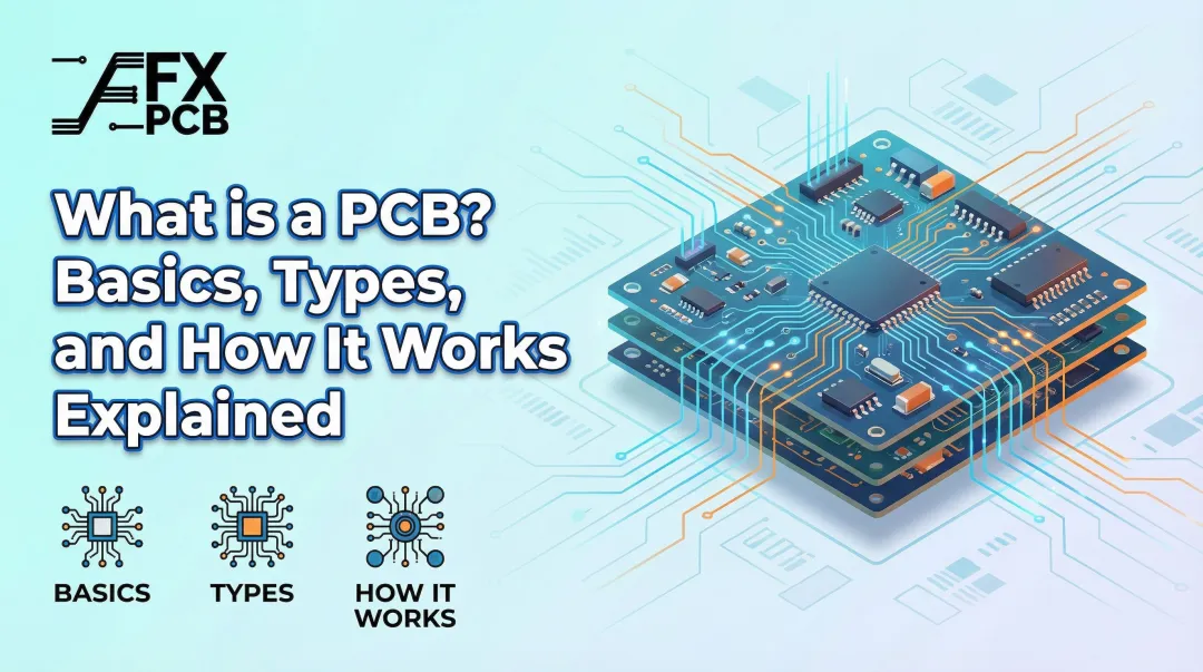
Introduction
Single-sided and double-sided PCBs power everything from LED drivers and calculators to automotive dashboards and industrial controllers. Choosing the wrong board type, though, can trigger signal failures, inflate manufacturing costs by 30–50%, or force rework cycles that push your market launch back by weeks.
PCB type directly impacts unit cost, routing complexity, thermal performance, and signal integrity. NASA research shows that design errors caught during testing cost 21x to 78x more to fix than those caught in the requirements phase. Board-type selection is a critical early call — and it should be driven by project requirements, not habit.
This guide breaks down both board types across cost, design complexity, thermal behavior, and ideal use cases so you can make that call with confidence.
Key Takeaways
- Single-sided PCBs feature copper traces on one side only; double-sided boards use both sides connected by plated vias
- Single-sided boards cost 30-50% less and suit simple, low-density circuits under 20 components
- Double-sided boards enable higher component density, better signal integrity, and improved thermal management
- Choose based on circuit complexity, form factor, signal speed, budget, and thermal demands
- Start with single-sided for cost-sensitive, simple designs; move to double-sided when density, speed, or heat dissipation push you past what one layer can handle
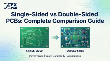
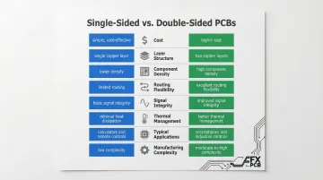
Single-Sided vs. Double-Sided PCBs: Quick Comparison
| Attribute | Single-Sided PCB | Double-Sided PCB |
|---|---|---|
| Cost | Lower cost / simpler manufacturing process | 30–50% higher cost; via drilling and layer alignment required |
| Layer Structure | One copper layer on single side | Copper layers on both sides connected by plated vias |
| Component Density | Low to medium; best for simple, low-component-count designs | High density / compact footprints |
| Routing Flexibility | Limited / requires jumper wires for trace crossovers | Flexible routing / traces cross layers via vias |
| Signal Integrity | Adequate for low-frequency (<100 MHz) | Better noise control / supports controlled impedance routing up to GHz-range signals |
| Thermal Management | Single-side heat dissipation | Dual-side heat distribution / thermal vias available |
| Typical Applications | LED drivers, calculators, power supplies, consumer appliances | Automotive ECUs, medical monitors, industrial PLCs, drone controllers |
| Manufacturing Complexity | Fast turnaround / 98%+ yield rates | Longer lead times / more rigorous inspection required |
What is a Single-Sided PCB?
A single-sided PCB consists of a single conductive copper layer laminated onto a non-conductive substrate—typically FR-4 fiberglass-epoxy. Components mount on one side, with copper traces etched on the same surface to create electrical pathways. The opposite side remains bare or displays labeling.
Manufacturing Process:
Single-sided boards follow a streamlined production path: copper lamination, photolithography, single-step chemical etching, and solder mask application. These boards contain no plated through-holes (PTH)—all drilled holes are non-plated, used only for component mounting or tooling. This eliminates electroless and electrolytic copper plating steps entirely, reducing manufacturing costs by 30-50% compared to double-sided variants.
Core Advantages:
- Cuts material costs through simplified, single-layer manufacturing
- Achieves yield rates consistently above 98% with faster fabrication cycles
- Simplifies inspection and troubleshooting—all traces visible on one layer
- Eliminates via drilling and layer alignment, reducing defect risk significantly
Key Limitations:
Single-sided boards restrict designers to low-to-medium component counts (typically under 15-20 components). Because traces cannot cross on a single layer, designers must use jumper wires or zero-ohm resistors to bridge intersecting nets. Each jumper adds approximately $0.02 to $0.10 in assembly costs for handling, installation, and inspection. If a design requires multiple jumpers, these cumulative costs can quickly exceed bare-board savings, making a double-sided board more economical.
Use Cases of Single-Sided PCBs
Single-sided PCBs account for nearly 19% of total PCB production by revenue ($4.87 billion in 2023), dominating cost-sensitive, high-volume applications. Common applications span several industries:
Consumer Electronics:
- Calculators (Casio fx-82MS)
- Remote controls (Roku RC-MC1)
- Basic LED drivers and power supplies
- Electronic timers and appliances
LED Lighting, Power Supplies & Instrumentation:
- Aluminum-backed PCBs for LED bulbs and strip lights (thermal conductivity up to 2.0 W/m·K)
- 5V USB wall chargers, low-wattage SMPS, and solar charge controllers handling low-frequency signals
- HVAC thermostats, environmental sensors, and digital multimeters where mass-market cost targets drive design
SFX PCB's free DFM (Design for Manufacturability) analysis helps designers confirm whether a single-sided layout is feasible for their specific circuit before committing to production—catching routing conflicts, component density issues, and potential jumper wire requirements early to avoid costly rework.
What is a Double-Sided PCB?
A double-sided PCB features conductive copper layers on both the top and bottom surfaces of the substrate, interconnected by plated through-holes (PTH) or vias. These copper-plated holes carry electrical signals between layers, enabling trace crossovers without physical jumper wires.
Manufacturing Process:
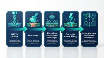
Double-sided boards require several additional steps beyond single-sided fabrication:
- CNC drilling to create via holes through the substrate
- Desmearing to remove resin residue from drilled hole walls
- Palladium-based catalyst application for electroless copper plating (depositing a 0.5–1.0 µm seed layer)
- Electrolytic copper plating using DC current, building hole wall thickness to 18–25 µm (per IPC-6012)
- Precise layer alignment and a second soldering pass for top-side components
These steps add both cost and lead time. At SFX PCB, standard lead times run 14 working days for aluminum-based boards and 16 working days for copper-based designs, with 24-hour expedited service available.
Core Advantages:
- Supports PIN densities above 1.0 per square inch, enabling denser component layouts in smaller footprints
- Routes traces across layers via vias, eliminating the need for jumper wires
- Enables controlled impedance routing for better signal integrity (SFX PCB holds ±10% impedance tolerance)
- Distributes heat across both sides through thermal vias and copper pours
Trade-offs:
- Costs run 30–50% higher per board due to via drilling, plating, and alignment
- Production and inspection take longer, with more rigorous quality checkpoints
- Design requires attention to via placement rules, annular ring sizing (4 mil minimum at SFX PCB), and stackup planning
- Two-sided component population increases troubleshooting complexity
Use Cases of Double-Sided PCBs
Double-sided PCBs dominate the 1-2 layer market with a 60% revenue share, driven by performance and density requirements across several demanding applications.
Automotive accounts for over 36% of global revenue in this segment, the largest share of any industry. ECUs, ADAS radar sensors, infotainment displays, and lighting systems all depend on double-sided layouts. The Continental ARS 4-B radar sensor, for instance, fits 76–77 GHz signal handling with microstrip antennas onto a 92×68 mm board.
Industrial control systems such as PLCs use modular, stacked double-sided construction — separating power and I/O boards from logic boards running 32-bit microcontrollers and Ethernet interfaces.
Medical monitoring devices including portable diagnostic instruments and vital sign monitors use double-sided layouts to isolate sensitive analog sensor inputs from digital communication lines. TI's AFE4403 pulse oximeter reference design is a well-known example.
Drone ESCs handling 20A–60A per motor rely on copper pours across both layers to distribute power and manage heat during rapid MOSFET switching.
Telecom and LED lighting hardware use double-sided routing to pack driver circuits and communication logic into tightly defined board footprints.
Single-Sided vs. Double-Sided: Which One is Right for Your Project?
Which board type fits your project depends on five concrete constraints. Work through each one to land on the right decision before your layout is locked in.
1. Circuit Complexity and Component Count
Choose Single-Sided When:
- Component count stays under 15-20 parts
- No trace crossovers exist in your layout
- Circuit operates at low frequencies (<50 MHz)
Choose Double-Sided When:
- PIN density exceeds 1.0 per square inch
- Design requires routing on multiple planes
- Trace crossovers would require multiple jumper wires
Reality Check: If your single-sided design needs more than 3-4 jumper wires, the cumulative assembly cost ($0.02-$0.10 per wire) will likely exceed the bare-board savings of avoiding a double-sided design.
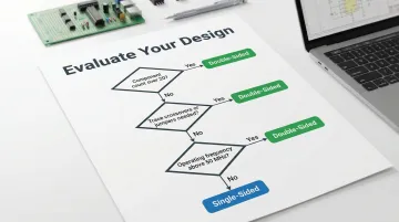
2. Form Factor and Size Requirements
Choose Single-Sided When:
- Board size can accommodate all components on one surface
- Physical space is not constrained
- Design can tolerate larger footprints
Choose Double-Sided When:
- Compact form factor is mandatory
- Components must fit in a small enclosure
- Vertical stacking of components is required
3. Signal Speed and Integrity Needs
The 1/10th Wavelength Rule: A trace must be treated as a transmission line (requiring controlled impedance and a continuous ground return path) when its physical length exceeds 1/10th of the signal's wavelength. For a 100 MHz signal with a 3ns rise time, this critical length is approximately 8 inches.
Choose Single-Sided When:
- All signal traces are shorter than the critical length
- Operating frequencies stay below 50 MHz
- EMI and crosstalk are not concerns
Choose Double-Sided When:
- Traces exceed critical length and require impedance control
- High-speed digital or RF circuits demand continuous ground planes
- Signal integrity is critical to product function
SFX PCB supports controlled impedance routing on double-sided boards with ±10% tolerance, suitable for most high-speed applications.
4. Production Budget and Volume
Choose Single-Sided When:
- Budget is a hard constraint
- High-volume production (10,000+ units) where per-unit cost dominates
- Simple consumer goods targeting mass markets
Choose Double-Sided When:
- Performance justifies the 30-50% cost premium
- Mid-to-low volume production where functionality matters more than unit cost
- Product pricing can absorb higher manufacturing costs
5. Thermal Management Demands
Choose Single-Sided When:
- Heat generation is minimal
- Single-sided aluminum base provides adequate thermal conductivity (up to 2.0 W/m·K)
- Components don't require aggressive heat dissipation
Choose Double-Sided When:
- High-power components generate significant heat
- Thermal vias and dual-sided copper pours are needed
- Operating temperatures exceed single-layer thermal capacity
Real-World Scenario Comparison
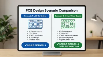
Scenario 1: Basic LED Controller for Consumer Appliance
- Component count: 12 parts (LED driver IC, resistors, capacitors, connectors)
- Signal frequency: DC to 1 MHz PWM
- Form factor: 50mm x 30mm with ample space
- Budget: $0.50 per board target at 50,000 units
- Thermal: Minimal heat from LED driver
Decision: Single-sided FR-4 board. No trace crossovers, low frequency, cost-sensitive application. Single-sided aluminum base if thermal dissipation becomes a concern.
Scenario 2: Motor Driver Board for Industrial Automation
- Component count: 45 parts (microcontroller, MOSFETs, gate drivers, sensors, communication ICs)
- Signal frequency: 20 MHz SPI, high-current PWM switching
- Form factor: 60mm x 40mm (space-constrained enclosure)
- Budget: $3.50 per board acceptable at 5,000 units
- Thermal: MOSFETs generate significant heat during switching
Decision: Double-sided FR-4 board with thermal vias. Component density requires dual-sided routing, high-speed signals need ground plane for integrity, thermal management demands dual-sided copper distribution.
When to Upgrade from Single-Sided to Double-Sided
Upgrade when your design hits any of these thresholds — each one signals that a single layer can no longer carry the design:
Routing Conflicts:
- Jumper wires required to resolve trace conflicts
- Component placement compromised to avoid crossovers
- Layout iterations repeatedly fail to route on single layer
Space Constraints:
- Board footprint cannot accommodate all components on one side
- Enclosure size forces tighter component packing
- Vertical height restrictions require components on both sides
Performance Issues:
- Signal integrity problems at target frequencies
- EMI/crosstalk exceeds acceptable levels
- Thermal management inadequate with single-sided heat dissipation
Component Requirements:
- BGA (Ball Grid Array) components requiring via fanout
- High-pin-count ICs demanding dense routing
- Mixed analog/digital circuits needing ground plane isolation
SFX PCB manufactures both single-sided and double-sided boards with 100% electrical testing on every bare board and free DFM analysis on every order, helping engineers validate their board-type decision before scaling to production. Submit your Gerber files for a no-obligation review within 24 hours.
Conclusion
Single-sided PCBs deliver proven cost efficiency and manufacturing simplicity for straightforward applications, holding a resilient 40% market share through 98%+ yield rates and dominance in LED lighting, power supplies, and consumer electronics. Double-sided PCBs unlock the routing flexibility, component density, and signal performance needed for advanced products in automotive, medical, and industrial sectors.
Your specific application requirements drive the decision. Component count, signal frequency, form factor constraints, budget, and thermal demands each pull the choice in a direction — and no single factor overrides the others.
Starting with a clear set of requirements and working backward to the board type is the most reliable path to a manufacturable, cost-effective design.
The board type you choose directly affects unit cost, time-to-market, rework risk, and long-term reliability. Getting that decision right early — ideally validated through DFM analysis before fabrication begins — prevents costly changes later in your development cycle.
Frequently Asked Questions
What is the difference between single-sided and double-sided PCBs?
Single-sided PCBs have copper traces and components on one side only, while double-sided PCBs feature traces and components on both sides connected by plated through-hole vias. This fundamental difference enables double-sided boards to support more complex circuits and higher component density without jumper wires.
What are the advantages and disadvantages of single-sided PCBs?
Single-sided PCBs offer 30-50% lower manufacturing cost, faster fabrication (5-9 days standard), and simpler troubleshooting since all traces are visible on one side. The trade-off is limited component density (under 20 components), no trace crossovers without jumper wires, and poor performance in circuits above 50 MHz.
What are the advantages and disadvantages of double-sided PCBs?
Double-sided boards pack more components into a smaller footprint, support controlled impedance (±10% tolerance), and distribute heat across both layers. The cost is 30-50% higher than single-sided, lead times run 14-16 days, and design complexity increases with via placement rules and annular ring sizing to manage.
Which is more expensive to manufacture: single-sided or double-sided PCBs?
Double-sided PCBs cost 30-50% more to manufacture, driven by additional CNC drilling, electroless and electrolytic copper plating for vias, precise layer alignment, and extended inspection. Assembly adds further cost through two-pass reflow soldering with separate stencils for each side.
Can single-sided PCBs be used for high-frequency applications?
Single-sided boards are not recommended for signals above 50-100 MHz — they lack a continuous ground plane for impedance control and are vulnerable to crosstalk and EMI. Once traces exceed 1/10th of the signal wavelength, a double-sided board with a ground plane is required.
When should I upgrade from a single-sided to a double-sided PCB?
Upgrade when your design needs jumper wires to resolve routing conflicts, when all components no longer fit on one side, or when signal integrity or thermal demands exceed single-layer limits. BGA components and any circuit requiring controlled impedance effectively require double-sided construction.