Introduction
A multilayer PCB passes visual inspection and even X-ray, yet fails in the field—intermittent electrical failures traced back to an internal layer misalignment or void invisible from the outside. This scenario plays out more often than most engineers realize. Field data from automotive suppliers reveals that up to 40% of "no-fault-found" returns trace back to hidden internal defects that AOI and X-ray missed entirely.
As multilayer PCBs grow in complexity — 4, 8, 12+ layers across automotive, medical, and aerospace applications — validating the internal layer stackup is no longer optional. It is the difference between a reliable product and a costly field failure.
The scale of adoption makes this especially urgent. 71% of new EVs integrate multilayer PCBs with 8 to 12 copper layers, driving a 58% growth in HDI PCB usage. The aerospace and defense multilayer PCB market is projected to reach $959 million by 2030, accounting for 96% of the sector's PCB market. Cross-section analysis addresses the gap non-destructive methods leave open — this guide covers the process, what it detects, and how to interpret results across common stackup configurations.
Key Takeaways
- Cross-section analysis physically exposes internal layer stackup to validate quality and detect hidden defects
- Reveals copper plating thickness, via integrity, and layer adhesion that X-ray and AOI cannot detect
- Applied across design validation, production QC, and failure analysis — each stage catching different classes of defect
- Detects delamination, solder voids, plating inconsistencies, and resin recession before they reach the field
- Reduces rework costs and ensures IPC-6012 compliance at critical production milestones
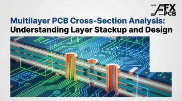
What Is Multilayer PCB Cross-Section Analysis?
Cross-section analysis (also called microsectioning) is a destructive PCB inspection technique in which a small sample is physically cut from the board, mounted in potting compound, ground, polished, and examined under a microscope to reveal the internal layer structure.
The process is formally defined by IPC-TM-650 Test Method 2.1.1, which establishes guidelines for preparing metallographic specimens to evaluate laminate system quality and plated structures.
Scope of Analysis
Cross-section analysis evaluates every structural element of the stackup at microscopic resolution not achievable through non-destructive methods:
- Copper layers (inner and outer)
- Prepreg dielectric layers
- Via barrels and plated through-holes (PTHs)
- Solder joints
- Surface finishes
Together, these structural elements tell a complete story about build quality. That story gets applied across three primary use cases:
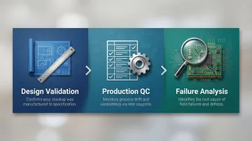
Three Primary Use Cases
Design Validation: Confirms the intended stackup was manufactured correctly. First article inspection verifies that dielectric thicknesses match impedance control calculations and copper weights meet current-carrying requirements.
Production QC: Catches process drift during a production run. Manufacturers use test coupons fabricated alongside production panels to perform destructive testing without sacrificing functional boards.
Failure Analysis: Investigates a failed or returned board to pinpoint the root cause. When field failures occur with unknown origins, cross-section reveals the internal defects responsible.
Why Cross-Section Analysis Is Critical for Multilayer PCB Stackup Validation
As layer counts increase, so does complexity and risk. A 12-layer board with blind and buried vias has dozens of internal interfaces where delamination, misregistration, or plating defects can occur, yet the board surface appears perfectly normal under standard inspection.
Cross-section analysis is how engineers confirm that what was designed is actually what was built — before a field failure makes that question urgent.
Direct Validation of Stackup Design Intent
Cross-section analysis directly validates that:
- Dielectric thicknesses match impedance control calculations
- Copper weights match current-carrying requirements
- Via structures connect the correct layers without shorts or opens
This ties quality assurance directly to electrical performance outcomes. Research from Polar Instruments shows that resin flow during lamination can shift differential impedance by 3.5 to 4.0 ohms, and etch taper variations can shift impedance by over 5 ohms.
Regulatory and Industry Requirements
Industries such as automotive (IATF 16949), aerospace (MIL-PRF-31032), and medical devices (ISO 13485) require documented evidence of internal PCB quality. Cross-section analysis is the accepted method for generating that evidence under IPC-6012 and IPC-A-600 standards.
For manufacturers holding ISO 13485 and IPC-A-610 Class 2/3 certifications — like SFX PCB — cross-section analysis is a routine production QC step, not an exception. It provides the documented, measurable evidence that regulated industries require before a board ships.
What a Cross-Section Reveals: Inside a Multilayer PCB Stackup
Copper Layer Thickness and Uniformity
Cross-section analysis measures actual copper thickness on each layer (inner and outer) and inside via barrels, verifying it matches the specified copper weight. Engineers often assume 1 oz/ft² copper guarantees exactly 35 µm of thickness. However, IPC-4562B allows up to a 10% manufacturing reduction, meaning base copper can legally be as thin as 31.31 µm.
IPC-6012F defines different plating thresholds based on application criticality — Class 3 imposes tighter limits than Class 2 across every metric:
| Feature | Class 2 Minimum | Class 3 Minimum |
|---|---|---|
| Hole Wall Plating (Average) | 20 µm (0.8 mil) | 25 µm (1.0 mil) |
| Surface Copper Plating | 20 µm (0.8 mil) | 25 µm (1.0 mil) |
| Plating Voids (Total) | 5% cumulative allowed | No multiple voids allowed |
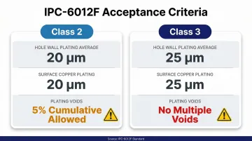
Uneven plating reduces current capacity and signal integrity. Class 3 boards strictly prohibit multiple plating voids within a single hole.
Dielectric Layer Integrity and Thickness
Cross-section measures prepreg and core dielectric thicknesses between each copper layer. These measurements are critical for controlled-impedance designs. A dielectric that is too thin or too thick shifts trace impedance away from the target value — commonly 50 Ω for high-speed signals — and directly causes signal integrity failures.
IPC-6012F lowered the default minimum dielectric spacing to 65 µm (2.56 mil) to accommodate laser-drilled microvias in HDI designs. However, resin flow into gaps during lamination alters the dielectric constant, requiring cross-section validation to measure the true pressed-out dielectric thickness.
Via and PTH Barrel Quality
Via barrels are examined for wall thickness uniformity, voids, cracks, and separation from the barrel wall. Blind and buried vias in HDI multilayer designs are especially difficult to inspect without destructive methods, making cross-section the only reliable verification method for via integrity.
Under thermal stress, the CTE mismatch between copper and epoxy resin concentrates stress at plating voids, leading to circumferential barrel cracks. A study using interconnect stress testing (IST) demonstrated that under extreme thermal cycling (up to 210°C), wear-out failures (barrel cracking) initiated as early as 128 cycles.
Layer-to-Layer Registration and Alignment
In a multilayer PCB, each inner layer must align precisely with adjacent layers during lamination. Cross-section reveals misregistration — layer shift during pressing — that can produce defects including:
- Via-to-pad misalignment that creates intermittent open connections
- Unintended short circuits between adjacent layers
- Reduced annular ring width that fails IPC minimum requirements
- Reliability degradation under thermal cycling in field conditions
Solder Joint and Intermetallic Bond Quality
Solder joint cross-sections reveal grain structure, intermetallic compound (IMC) thickness, voids, cold joint indicators, and wetting conditions at the pad interface—details essential for assessing long-term joint reliability under vibration and thermal stress in automotive and industrial applications.
How Multilayer PCB Cross-Section Analysis Works – Step by Step
The process must be performed carefully to avoid introducing artifacts (scratches, edge rounding, smearing) that distort findings. Rushing through polishing is one of the most frequent causes of inaccurate results.
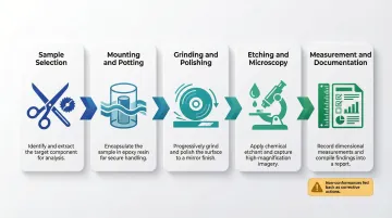
Before diving into each step, here's what the process covers at a glance:
- Sample selection — test coupon or failed board region
- Mounting and potting — encapsulation for geometry protection
- Grinding and polishing — progressive abrasive sequence
- Etching and microscopy — contrast enhancement and imaging
- Measurement and documentation — comparison against IPC-6012 acceptance criteria
Step 1 – Sample Selection and Sectioning
Samples are either taken from dedicated test coupons (fabricated as extensions of the production panel under IPC-2220 standards, sharing the same material and layer structure) or from a failed/suspect board region. The sample is cut using a precision diamond saw.
Test coupons allow destructive testing without sacrificing functional boards — an essential advantage for production quality control.
Step 2 – Mounting and Potting
The sample is encapsulated in a polymer or epoxy potting compound to protect the delicate cross-section geometry during grinding. IPC-TM-650 2.1.1 mandates a maximum cure temperature of 93°C (200°F) to prevent thermal stress damage during curing.
Alignment during potting is non-negotiable. Misaligned samples expose the wrong plane and lead to inaccurate layer measurements.
Step 3 – Grinding and Polishing
The process follows a progressive polishing sequence:
- Coarse silicon carbide paper (180 to 1200 grit) to expose the plane of interest
- Fine abrasives (down to 0.3-0.04 µm colloidal silica or 1.0-6.0 µm diamond powder) to achieve a scratch-free surface
The grinding accuracy must ensure the viewing area of the PTH is within 10% of the drilled hole diameter to guarantee measurements are taken at the true centerline. Edge rounding must be minimized to preserve accurate copper and dielectric thickness measurements.
Step 4 – Etching (Optional) and Microscopy
Micro-etching solutions enhance contrast between copper layers, intermetallic zones, and dielectric materials before imaging. Two primary inspection instruments are used:
- Metallograph (optical microscope, up to 1000× magnification) for standard layer and plating measurements
- Scanning Electron Microscope (SEM) for higher-resolution analysis of grain structure, cracks, and compositional mapping (via EDX)
IPC-TM-650 2.1.1 requires a minimum of 100× magnification for examination.
Step 5 – Measurement, Documentation, and Action
Key measurements taken include:
- Dielectric thickness per layer
- Copper plating thickness (basic, plated, and total)
- Barrel wall thickness
- Void percentage in vias
- Solder joint dimensions
Results are compared against IPC-6012 acceptance criteria and the original design stackup specification. Non-conformances are documented and fed back into the fabrication process as corrective actions — turning cross-section analysis into a continuous process improvement tool rather than a one-time quality gate.
Key Defects Identified in Layer Stackup Through Cross-Section Analysis
Delamination and Voids Between Layers
Delamination—separation of copper from prepreg or between dielectric layers—typically results from inadequate lamination pressure or temperature, moisture contamination in the prepreg, or thermal cycling stress. Cross-section reveals these as visible gaps or air pockets at layer interfaces, which act as stress concentration points and eventually cause electrical failure.
A comprehensive NASA GSFC failure analysis study evaluating 882 PCB coupon submissions from 2015 to 2017 found that inner-layer separations/inclusions and plating separations consistently ranked among the top 5 severity nonconformances from PCB suppliers.
Inner Layer Misregistration and Trace Over-Etching
Misregistration (layer shift during lamination) and over-etching (excessive copper removal during inner layer patterning) are revealed by measuring the actual position of inner layer traces relative to via pads and checking trace width against design spec. Both defects can cause high-frequency signal integrity issues or outright opens that only manifest under thermal stress.
Via Barrel Defects (Cracks, Voids, Separation)
Specific via defects that cross-section identifies include:
- Knee cracks at the via entry/exit points due to thermal cycling
- Mid-barrel voids from inadequate electroplating
- Barrel separation (the plated copper pulling away from the hole wall)
These are especially critical in boards that experience wide temperature swings, such as automotive ECUs or outdoor telecom equipment.
Resin Recession and Epoxy Smear
Resin recession (dielectric material pulling back from the via barrel wall) and epoxy smear (dielectric material smeared onto via barrel copper during drilling) both compromise inter-layer electrical connections and are impossible to detect without cross-sectioning.
Epoxy smear from poorly tuned drilling parameters causes high-resistance vias that pass initial electrical test but fail under load. IPC-6012 requires complete removal of epoxy smear, yet it remains undetectable by X-ray or AOI.
How SFX PCB Can Help
SFX PCB has over 15 years of experience producing complex multilayer boards for medical, automotive, aerospace, and industrial automation customers. Their ISO 13485 certification and IPC-A-610 Class 2/3 compliance mean the production QC framework is built around the same acceptance criteria that cross-section analysis validates against.
Multi-Stage Quality Assurance Approach
SFX PCB implements a multi-stage quality verification process:
- Free DFM (Design for Manufacturability) analysis on every order to catch stackup design issues before fabrication begins
- 100% electrical testing on every bare board
- Advanced inspection using AOI and X-ray equipment
- Cross-section analysis available as part of quality verification for high-reliability orders
- Six-stage inspection process incorporating SPI, 3D AOI, and X-ray inspection
The company's multilayer PCB capabilities span 4-layer, 6-layer, and 8-layer standard offerings, with custom configurations up to 30 layers for complex multilayer designs. SFX PCB produces boards with blind vias and buried vias for HDI multilayer designs, supporting the advanced via structures that are especially difficult to inspect non-destructively.
Seamless Prototype-to-Production Scaling
SFX PCB's ability to scale from prototype to high-volume production without a supplier change means the same stackup and process parameters validated at the prototype stage (including cross-section verification) carry directly into mass production. Production maintains ±0.05mm precision across all stages, eliminating process drift as volumes increase. Three controls reinforce this consistency:
- Layer-to-layer alignment verification at each fabrication stage
- ERP-based production tracking linking prototype specs directly to production runs
- Systematic QC checkpoints ensuring stackup parameters don't shift between volumes
Frequently Asked Questions
Is PCB cross-section analysis a destructive test?
Yes, cross-section analysis is a destructive method—the sampled portion of the board or test coupon cannot be used afterward. Test coupons fabricated alongside the production panel allow manufacturers to perform cross-section analysis without scrapping functional boards.
What is the difference between PCB cross-section analysis and X-ray inspection?
X-ray is a non-destructive method that shows 2D projection images of internal features (useful for BGA voids or large voids). Cross-section analysis physically exposes the stackup, providing precise measurements of copper thickness, dielectric dimensions, and microstructural details that X-ray cannot resolve.
What IPC standards apply to multilayer PCB cross-section analysis?
Two standards govern this process:
- IPC-6012: Qualification and performance specification for rigid boards — defines acceptance criteria for copper thickness, via quality, and dielectric integrity
- IPC-A-600: Acceptability of printed boards — provides visual acceptance criteria for cross-section evaluation
When should you request cross-section analysis for a multilayer PCB design?
Request cross-section analysis in these situations:
- First article inspection of a new multilayer design to validate the stackup
- When a production process parameter changes (new material lot, drilling or plating adjustment)
- Whenever a field failure occurs and the root cause is unknown
What layer stackup defects can only be found through cross-section analysis and not by other inspection methods?
Several defects are only detectable through cross-section analysis:
- Inner layer misregistration
- Barrel separation in buried vias
- Epoxy smear and resin recession
- Intermetallic compound thickness in solder joints
- Dielectric delamination at internal layer interfaces