Ceramic PCB

Complete Guide to the Manufacturing Process of Ceramic PCB
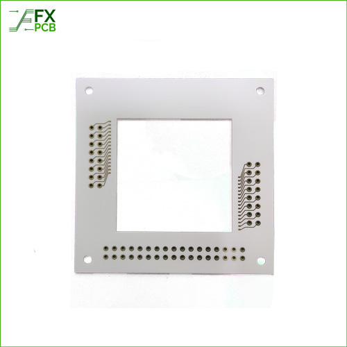
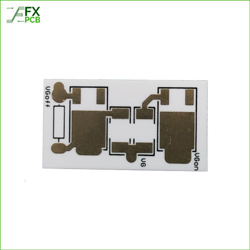
The world of electronics manufacturing is fast-paced, evolving, and intricate. Among others, ceramic Printed Circuit Boards have emerged as a cutting-edge solution.

A Ceramic PCB Manufacturer provides unique solutions, effectively addressing the increasing demands for higher performance, longer lifespan, and enhanced thermal management. This article delves into the fascinating world of ceramic PCB manufacturing, outlining this technological marvel’s process, benefits, and applications.

Table of Contents

Our Recommended Ceramic PCB

Ceramic PCB

FX PCB can provide the ALN(Aluminum oxide) and AIO203(Aluminum Nitride) Ceramic PCB, we can make ENEPIG, ENIG, Immerison silver surface,you can check the material datesheet and our capability from the below tables.

The ceramic circuit board has the following characteristics: high-temperature resistance, high electrical insulation, low dielectric constant, low dielectric loss, high thermal conductivity, good chemical stability, and the thermal expansion is almost can be coefficients of components.

Ceramic PCB is actually made of electronic ceramic materials and can be made into various shapes.

From Silicon to Ceramic: A Paradigm Shift

Traditionally, PCBs were made of materials like FR4 or CEM, types of fiberglass that are affordable but have limitations regarding heat dissipation, thermal expansion, and frequency performance. These shortcomings became pronounced with the miniaturization trend and higher operating frequencies, pushing manufacturers towards more suitable materials; Ceramics.

Ceramics, known for their exceptional thermal conductivity, electrical insulation, and chemical stability, offer a promising alternative for manufacturing PCBs. Suitable for high-power applications of electronics, they are durable at high temperatures and probably the most common reason for being a common alternative to standard FR4 boards. But how are ceramic PCBs manufactured? Let’s find out.

Step 1: Ceramic Substrate Creation

The first step in the ceramic PCB manufacturing process involves creating the ceramic substrate. High-purity alumina or aluminum nitride powders are the primary materials used. They are mixed with organic binders and solvents to create a viscous paste. This paste is then subjected to tape casting or a similar technique to produce a thin sheet.

Following this, the ceramic sheet undergoes a process known as debinding. Here, the organic materials are slowly removed by heating, leaving behind a porous ceramic body. Finally, the substrate is sintered in a kiln at high temperatures, resulting in a dense, robust ceramic plate ready for the next stage.

Step 2: Metalization

In the fascinating journey of ceramic PCB manufacturing, the process of metalization comes across as a significant milestone. Think of it as creating a conductive roadmap on the blank canvas of the ceramic substrate.

Picture an artist carefully creating a masterpiece. The process uses a technique akin to screen-printing, where a design is meticulously transferred to another surface. The metal paste is gently spread over the ceramic, tracing the blueprint of the desired circuit paths.

Once the initial application is complete, the ceramic substrate literally endures a baptism by fire. It’s subjected to high-temperature firing, which transforms the applied metal paste into a conductive layer. During this heat treatment, the metal bonds with the ceramic, forming the crucial foundation for the circuit connections. This layer will carry the lifeblood of the device – electrical signals.

Step 3: Circuit Patterning

After metalization comes the process of circuit patterning. It’s time to breathe life into the previously laid conductive paths. The actual circuit design is etched onto the metalized substrate, creating the exact pattern of the intended electronic design.

The process starts by applying a layer of photoresist onto the metal surface. Think of the photoresist as a protective barrier, a shield that selectively safeguards certain areas during the etching process. The photoresist-covered substrate is then exposed to UV light, but not before placing a mask that outlines the desired circuit design.

Then comes the etching – a process reminiscent of a sculptor chiseling away unnecessary portions from a block of stone. The unexposed areas are chemically etched away, leaving behind a beautifully defined circuit pattern. Like an intricate piece of art, each line, and each pathway is part of a complex network, ensuring that the PCB functions as per the designed intent.

Step 4: Layer Stacking and Via Drilling

The process continues with layer stacking for the more complex multilayer ceramic PCBs. Multiple ceramic layers, each with its distinct circuitry, are carefully aligned and stacked.

Alongside stacking, another crucial process takes place – via drilling. Vias are like elevators connecting the different levels of our imaginary building. They are small holes drilled through the layers, allowing for vertical connections between different circuit planes.

Once the layers are stacked and vias drilled, the entire assembly undergoes another round of firing. This high-temperature ordeal fuses the layers together, solidifying the multilayer ceramic PCB.

Step 5: Final Metalization and Plating

Even after stacking and firing, the ceramic PCB isn’t quite ready. It requires another layer of metal, a final act of metalization. This layer, usually of copper, silver, or gold, is meant to improve electrical conductivity.

Additionally, this final metal layer plays a crucial role in enhancing the solderability of the PCB. It ensures that components can be securely attached, standing up to the operating pressures and providing a long-lasting connection.

Step 6: Inspection and Testing

No Ceramic PCB Manufacturer would complete the manufacturing process without the all-important stage of inspection and testing. The manufacturer’s commitment to quality assurance is the last hurdle before the PCBA is ready for deployment.

During this phase, the finished PCBs are visually inspected for any possible defects. A meticulous eye scans for imperfections, ensuring that what goes out of the factory doors is nothing short of perfection.

Beyond visual inspection, the PCBs are put through rigorous electrical tests. The tests check for continuity and the isolation of circuits, a sort of dress rehearsal before the performance. This way, the Ceramic PCB Manufacturer ensures that every PCB shipped out is functionally flawless and ready to power the electronics of tomorrow.

ceramic pcb 2

The Value Proposition of Ceramic PCBs: A Game Changer

With their exceptional properties, ceramic PCBs are taking over high-performance electronics applications. Their low coefficient of thermal expansion improves reliability under high operating temperatures. Moreover, ceramic PCBs offer superior electrical performance, especially at high frequencies, making them a preferred choice for RF and microwave applications.

Ceramic PCBs offer a path forward in a world where electronic devices continue to shrink while their power and complexity grow. They make it possible for devices to run hotter, faster, and longer without succumbing to the limitations of traditional PCB materials.

Bottom Line

The science of ceramic PCB manufacturing, therefore, is more than just a process – it’s the pathway to the future of electronics. Embracing this transformative technology will no doubt pave the way for unprecedented advances in the world of electronics manufacturing. 

When it comes to Ceramic PCB suppliers in China, few can compare to FX PCB, which is at the front of this movement. Because we care about satisfying our clients, we produce both single-layer and multilayer printed circuit boards (PCBs).

Contact us for more details: https://sfxpcb.com/contacts/

Peter Gong
Peter Gong

I am Peter Gong. I have been working in PCB and PCBA industry for 15+ years now. I have been a part of the PCB revolution with my dedication to circuit board technologies and creative ideas. I write in FX PCB to impart my knowledge on PCB and PCBA for all circuit board lovers, manufacturers, and users.

Ceramic PCB

Ceramic PCB: Its Materials, Types, Benefits and Drawbacks

This digital age that we are fortunate to be a part of, has been built on a myriad of breakthroughs and developments. Underneath all these accomplishments lie the unsung heroes of technology – Printed Circuit Boards (PCBs). Imagine these PCBs as the silent veins of electronics, circulating life in the form of electrical signals. In their many avatars – Ceramics being one of the major ones, they help bring to life a diverse array of gadgets that we use daily. 

A Ceramic PCB is a type of PCB that utilizes ceramic as its base material. Ceramics have the capability to be electrically expended, can dissipate heat, and electrical insulation. These attributes enable Ceramic PCBs to operate in extreme conditions where other materials may fail and in industries like medical equipment, aerospace, etc. 

Let’s take a deep dive into the realm of Ceramic PCBs, uncovering the materials they are made of, the various types that exist, their impressive benefits, and the drawbacks that we must cautiously tread around.

Table of Contents

Our Recommended Ceramic PCB

Ceramic PCB

FX PCB can provide the ALN(Aluminum oxide) and AIO203(Aluminum Nitride) Ceramic PCB, we can make ENEPIG, ENIG, Immerison silver surface,you can check the material datesheet and our capability from the below tables.

The ceramic circuit board has the following characteristics: high-temperature resistance, high electrical insulation, low dielectric constant, low dielectric loss, high thermal conductivity, good chemical stability, and the thermal expansion is almost can be coefficients of components.

Ceramic PCB is actually made of electronic ceramic materials and can be made into various shapes.

Materials Used in Ceramic PCB

When we talk about ceramic printed circuit boards, or PCBs, the “ceramic” term can include a wide range of materials. Each one comes with its unique characteristics that make it a good fit for certain uses. Here are the major three materials used:

Alumina, or Al2O3

Alumina, or Al2O3, is the ceramic you’ll find most often in PCBs. Its popularity comes from its easy availability and cost-friendliness. It strikes a decent balance between thermal conductivity and electrical insulation properties with 24-28 W/mK conductivity.

Aluminium Nitride, or AlN

Aluminium Nitride, or AlN, is a go-to choice when you need top-notch thermal conductivity. With a thermal conductivity score of 170-230 W/mK, it’s a champ at getting rid of heat and keeping electronics functioning properly. 

Beryllium Oxide, or BeO

Beryllium Oxide, or BeO, outperforms all the other ceramics when it comes to thermal conductivity, achieving between 250-325 W/mK. But, it’s not used as widely because it’s toxic. Working with BeO requires a lot of safety precautions, which drives up manufacturing costs.

Types of Ceramic PCBs

There are a few different kinds of PCBs out there, and each has its strengths:

  1. Thick Film Ceramic Printed Circuit Boards are made by screen printing a conductive paste onto the ceramic base. Then, the board is fired at high temperatures to make the paste hard. They’re a cost-friendly choice and work well for mass production.
  2. Thin Film Ceramic Printed Circuit Boards are created by vapor depositing the conductive material onto the ceramic base. They’re more precise and perform better than Thick Film Ceramic PCBs, but they’re also more complex and expensive to produce.
  • Direct Copper Bonded (DCB) Ceramic Printed Circuit Boards are made by bonding copper right to the ceramic base. This technique results in top-tier thermal conductivity, which makes these PCBs a great fit for applications that demand a lot of power.
Ceramic PCB

Benefits of Ceramic Printed Circuit Boards

So, what makes Ceramic PCBs the rising star in the world of electronics? Here, we shed light on some of the key benefits that make them a popular choice:

High Thermal Conductivity

The word ‘ceramic’ often brings to mind images of pottery baking in a kiln. But this material, famed for withstanding high temperatures in a potter’s kiln, could play a pivotal role in electronic devices. With an inherent high thermal conductivity, Ceramic PCB is quite the master at heat management. They pull off a spectacular balancing act, keeping electronic components cool and ensuring the device’s longevity. It’s like having an in-built air conditioning system that works relentlessly to prevent overheating.

Electrical Insulation

When you’re working with electronics, safety is paramount. One wrong connection, and you might end up with a gadget that’s more ‘shocking’ than functional. Enter Ceramic Printed Circuit Boards, with their superior electrical insulation. Much like a conscientious electrician, they diligently prevent any unwanted flow of current, safeguarding your device from short circuits and maintaining overall stability.

Thermal Expansion Coefficient

Ever noticed how a sidewalk has gaps between the slabs of concrete? These are cleverly designed to allow the material to expand and contract without causing cracks. Similarly, Ceramic PCBs have a thermal expansion coefficient that’s close to silicon, a common semiconductor material. This similarity allows them to handle the heat-induced expansion and contraction of components efficiently, thus reducing mechanical stress and offering a harmonious work environment for the electronic components.

Resistance to Harsh Environments

Thanks to their chemically inert nature and resistance to extreme temperatures, Ceramics PCBs are like electronic explorers, adept at operating smoothly in harsh environments. Whether it’s the heat of an automotive engine or the freezing vacuum of outer space, these PCBs can handle it all.

High Frequency Performance

In the electronic world, maintaining signal integrity is crucial for the device to function properly. Thanks to their low signal loss, Ceramic PCBs ensure smooth performance, even at high frequencies. It’s like having a sound technician right inside your device, ensuring that the performance remains pitch-perfect.

Miniaturization

As we move towards an era of sleek, compact gadgets, space management has become more important than ever. These Printed Circuit Boards’ high component density, enable the creation of smaller and lighter devices without compromising on performance. It’s like having a talented architect who makes the best possible use of limited space.

Drawbacks of Ceramic PCBs

Despite the numerous advantages of Ceramic PCBs, there are a few drawbacks to consider:

  • Cost: Ceramic Printed Circuit Boards are typically more expensive to produce than their counterparts made from materials like FR4 or CEM1, expensive materials, and complex processes.
  • Brittleness: Ceramics, though excellent at withstanding high temperatures, possess a noticeable fragility. They can easily crack or shatter under physical pressure, which can pose problems during the assembly phase or if the final product is expected to face any kind of rough handling.
  • Design Limitations: Designing Ceramic Printed Circuit Boards requires a great deal of thought and precision because of the distinct attributes of the ceramic material. Once the PCB is produced, making design modifications can be a tough task.

If you are looking for a manufacturer with superior processing of Ceramic PCBs, FX PCB is the best in the market. We choose automated processing of ceramic manufacturing that gives us leverage over our competitors. Get the best quality PCBs from FX PCB. Visit here: https://sfxpcb.com/ 

Peter Gong
Peter Gong

I am Peter Gong. I have been working in PCB and PCBA industry for 15+ years now. I have been a part of the PCB revolution with my dedication to circuit board technologies and creative ideas. I write in FX PCB to impart my knowledge on PCB and PCBA for all circuit board lovers, manufacturers, and users.

Ceramic PCB

Ceramic PCB: A Detailed Material Property Comparison

When we think about PCBs, we often picture the traditional FR-4 (Fiberglass Reinforced Epoxy Laminated Sheets) due to its widespread use. However, as the world of electronics constantly evolves, materials that were once on the fringe have started to gain prominence. One such material is the Ceramic PCB. Let’s dive deep into this intriguing material and explore the characteristics that make it a noteworthy competitor in the realm of PCBs.

Table of Contents

Our Recommended Ceramic PCB

Ceramic PCB

FX PCB can provide the ALN(Aluminum oxide) and AIO203(Aluminum Nitride) Ceramic PCB, we can make ENEPIG, ENIG, Immerison silver surface,you can check the material datesheet and our capability from the below tables.

The ceramic circuit board has the following characteristics: high-temperature resistance, high electrical insulation, low dielectric constant, low dielectric loss, high thermal conductivity, good chemical stability, and the thermal expansion is almost can be coefficients of components.

Ceramic PCB is actually made of electronic ceramic materials and can be made into various shapes.

Brief Material Comparison

Exploring the necessity of Ceramic PCBs calls for a thorough understanding of the constraints associated with conventional materials. Traditional PCB materials like FR-4 have been foundational in electronics, providing consistent performance and cost-effectiveness. However, inherent drawbacks such as low thermal conductivity, limited electrical insulation, and restricted temperature endurance hinder their utilization in high-stakes, high-performance applications.


This is where
Ceramic PCB stride into the spotlight. They embody advanced characteristics that overcome the limitations of their conventional counterparts. They exhibit high thermal conductivity, exceptional electrical insulation, and robust temperature endurance – traits that arm them for high-frequency, high-power, and high-temperature operations. The superiority of Ceramic PCBs is unveiled upon further examination of their physical properties, fabrication process, and application range.

Fabrication Process

The fabrication of Ceramic PCBs follows a unique method known as the LTCC (Low-Temperature Co-fired Ceramic) or HTCC (High-Temperature Co-fired Ceramic) processes. These methods involve multiple layers of ceramic and metal being co-fired at high temperatures to produce a monolithic block that forms the final product. The co-firing process, although more intricate and complex than the traditional PCB manufacturing methods, offers robustness and longevity to the final product, allowing the Ceramic PCB to sustain its performance under harsh conditions.

Detailed Material Property Comparison

Thermal Conductivity: When any particular thing or substance (material) has the ability to conduct heat, it can be labeled as having properties of thermal conductivity. It’s particularly critical in the realm of PCBs because electronic components naturally generate heat when in operation. 

Their thermal conductivity isn’t just better; it’s in a league of its own, ranging from 20-300 W/m.K. With this dramatically heightened thermal conductivity, Ceramic PCBs don’t just inch ahead; they leap ahead, proving themselves to be the ideal candidates for applications where heat isn’t just a by-product, but a significant challenge to address.

Electrical Insulation: Next up is Electrical Insulation, another vital characteristic for any PCB material. A good electrical insulation acts as a barrier to prevent electrical current from traveling in unintended directions, reducing the likelihood of fires and other malfunctions caused by short circuits. Because they are not conductive, ceramic PCBs perform exceptionally well in this application. This inherent electrical insulation makes them especially suitable for applications that require both high-frequency operation and top-notch insulation.

Temperature Endurance: Another crucial trait of PCB materials is Temperature Endurance. As electronic components generate heat during operation, a PCB material needs to be capable of withstanding significant heat without its properties being adversely affected. This is where Ceramic PCBs really come into their own. Their superior temperature endurance means they can comfortably weather high operating temperatures that might cause other materials to falter.

Mechanical Strength: Apart from these features, they also display excellent Mechanical Strength, primarily due to their monolithic structure. This feature results in a robust and sturdy PCB that is less likely to succumb to physical damage, making them a particularly good choice for applications where durability is paramount.

Coefficient of Thermal Expansion (CTE): CTE is another significant factor, especially for PCBs that must operate in varying temperatures. This property is a measure of how much a material expands or contracts with changes in temperature. It’s an especially important consideration for PCBs that need to operate in environments with wide temperature fluctuations. A lower CTE means the material will remain stable under these changing conditions, thereby preventing the creation of mechanical stress on the components. Ceramic PCBs boast a low CTE, similar to silicon, making them a fantastic choice for applications that experience varying temperatures.

Ceramic PCB

Applications of Ceramic PCBs

The formidable properties of Ceramic PCBs have found their way into an array of sophisticated industries. They are significantly deployed in LED lighting systems, where effective heat dissipation – courtesy of their high thermal conductivity – is paramount. Furthermore, high-frequency gadgets such as RF and microwave circuits utilize Ceramic PCBs due to their low dielectric constant and loss factor, ensuring optimal performance.

Additionally, Ceramic PCBs are a perfect match for industries such as aerospace and automotive, where electronics are subjected to harsh, demanding operating conditions. The high temperature endurance of Ceramic PCBs renders them resilient in these extreme environments, offering stable performance even under stress.

Thus, the variety of applications and sectors benefitting from Ceramic PCBs is vast, which emphasizes their inherent versatility and durability. As the need for electronics capable of performing under high-demanding conditions continues to rise, Ceramic PCBs are poised to rise in prominence and ubiquity.

Conclusion

In the fascinating world of electronics, materials often make a world of difference. And as we see, Ceramic PCBs truly stand out due to their exceptional properties. Their high thermal conductivity, excellent electrical insulation, superior temperature endurance, and strong mechanical strength make them ideal for challenging applications. Now, every PCB has it’s own place, whether traditional or ceramic, and nobody can replace the other. However, as the technology evolves, Ceramic PCBs are surely getting ahead in the race to traditional ones due to their high technology and benefits. 

As we reflect on the exceptional attributes and far-reaching applications of Ceramic PCBs, it’s evident that the material’s future is both bright and promising. However, effectively harnessing these benefits requires skilled, reliable, and experienced manufacturing – something that isn’t easy to find.

Fortunately, at FX PCB, we are adept at turning this complex process into a seamless experience. We’re a leading manufacturer of PCBs of all kinds, based in China. Our proficiency extends beyond conventional PCB materials, and we excel in producing high-grade Ceramic PCBs. We thrive in delivering excellent customer service and promise to guide you every step of the way

To get more insight and details on our PCB products, click here.

Peter Gong
Peter Gong

I am Peter Gong. I have been working in PCB and PCBA industry for 15+ years now. I have been a part of the PCB revolution with my dedication to circuit board technologies and creative ideas. I write in FX PCB to impart my knowledge on PCB and PCBA for all circuit board lovers, manufacturers, and users.

Copper coin pcb

Introduction of the Ceramic PCB Manufacturing Process

The demand for low-power, high-performance devices keeps rising as we progress farther into the digital age. With traditional printed circuit boards (PCBs) increasingly falling short of the escalating demands, Ceramic PCBs have emerged as a promising alternative. Notably, the innovative manufacturing process adopted by leading Ceramic PCB Manufacturers is both fascinating and transformative. 

They are a type of PCB made from ceramics, which are non-metallic, inorganic, and often crystalline solids created through heat. Ceramics bring significant benefits over traditional materials used in PCBs, such as FR4 or metal core.

Table of Contents

Our Recommended Ceramic PCB

Ceramic PCB

FX PCB can provide the ALN(Aluminum oxide) and AIO203(Aluminum Nitride) Ceramic PCB, we can make ENEPIG, ENIG, Immerison silver surface,you can check the material datesheet and our capability from the below tables.

Ceramic PCB is actually made of electronic ceramic materials and can be made into various shapes.

The ceramic circuit board has the following characteristics: high-temperature resistance, high electrical insulation, low dielectric constant, low dielectric loss, high thermal conductivity, good chemical stability, and the thermal expansion is almost can be coefficients of components.

Order Now Ceramic PCB

The Role of a Ceramic PCB Manufacturer

A Ceramic PCB Manufacturer‘s responsibility extends far beyond simply churning out Ceramic PCBs. They undertake extensive research and development efforts to continually enhance the manufacturing process and explore new ceramic materials that deliver improved PCB performance.

Furthermore, they serve as crucial advisors to electronic design engineers, helping them understand Ceramic PCBs’ unique properties and advantages. This collaborative relationship between manufacturers and engineers is fundamental in optimizing the application of Ceramic PCBs across a multitude of industries, from telecommunications and automotive to medical and aerospace industries.

Decoding the Ceramic PCB Manufacturing Process

The manufacturing process of Ceramic PCBs is multi-tiered and complex. It essentially involves several stages, starting from raw material preparation to the finished product. 

1. Raw Material Preparation

The creation of a Ceramic PCB is akin to crafting a piece of art; it all starts with choosing the right materials. The initial stage of preparation requires various ceramics, such as alumina, aluminum nitride, or silicon carbide. The choice of ceramic used largely depends on the final application of the Ceramic PCB. Each of these materials brings unique properties to the table – for instance, alumina offers excellent electrical insulation, while silicon carbide has high thermal conductivity. Ceramic powders are then meticulously combined with organic binders and a variety of other additives to form a pliable and workable mixture. This process is crucial because the composition of this mixture determines the PCB’s physical and electrical properties.

2. Green Sheet Formation

Once the initial ceramic mixture is ready, it is then transformed into thin, flexible sheets, endearingly known as ‘green sheets.’ The sheets owe their flexibility to the organic binders used in the mixture, which allow the ceramic powder to be rolled out smoothly. Despite their delicate appearance, these sheets are robust and form the substrate of the Ceramic PCB. Their malleability and strength make them the ideal core building block for multi-layer Ceramic PCBs, which are the industry standard in high-tech applications.

3. Circuitry Printing

With the green sheets prepared, the manufacturing process shifts gears to the critical stage of circuitry printing. Here, a thick film of metallization paste, commonly gold or silver, is diligently screen printed onto the green sheet. This paste follows the carefully planned circuit design, effectively forming the electric pathways of the PCB. Any discrepancies in circuit printing can result in performance degradation or, in worst cases, the total failure of the PCB.

4. Laminating and Cutting

Following the intricate process of circuitry printing, the focus then turns to laminating and cutting. During this stage, the printed green sheets are methodically stacked layer upon layer, giving birth to the multi-layered structure that’s typical of a Ceramic PCB. It’s essential to align these sheets perfectly to maintain the integrity of the circuit design throughout the layers. Once the stacking is complete, they’re laminated under high pressure to ensure a secure and compact stack. The stack is then cut into the required shape and size, bringing us one step closer to the finished Ceramic PCB.

5. Sintering

Now comes the transformative phase – sintering. This process involves heating the laminated and cut Ceramic PCBs in a carefully controlled environment. The temperature, set below the melting point of ceramics, prompts the particles within the green sheets to bond together, forming a dense and rigid ceramic structure. During sintering, the organic binders that once provided flexibility to the green sheets evaporate, leaving behind a highly robust ceramic body etched with conductive traces.

6. Inspection and Testing

Once the sintering process completes its magic, the nearly finished Ceramic PCBs undergo a stringent quality assurance phase. Much like any reputable Ceramic PCB Manufacturer like FX PCB there’s a strong emphasis on quality control that oversees this process. It involves rigorous testing to evaluate the PCBs for mechanical robustness, electrical performance, and thermal properties, ensuring that they meet the exacting standards of the industry. If any PCB is found lacking, it is promptly rejected. This intense scrutiny helps ensure that only the best and most reliable Ceramic PCBs make it into the hands of the end-users.

Ceramic PCB Manufacturing Process

Technology Enhancements in Ceramic PCB Manufacturing

As we unravel the mesmerizing manufacturing process of Ceramic PCBs, it’s essential to shine a light on the instrumental role of technology in shaping this process. The evolving landscape of PCB manufacturing is being significantly influenced by advancements in technology. Consequently, Ceramic PCB Manufacturers are increasingly harnessing these technological leaps to enhance production quality and efficiency.

Computer-aided design (CAD) systems, for instance, play a pivotal role in the circuitry printing phase. These software tools allow manufacturers to design intricate circuit layouts with a high degree of precision. They also enable automated testing of the designs, thereby identifying potential issues even before the first layer of metallization paste is applied to a green sheet.

Similarly, sophisticated machinery and equipment underpin the laminating and cutting processes, ensuring the highest level of accuracy and uniformity across all PCB layers. It’s a testament to the technological prowess of the industry that even the minutest of details can be replicated perfectly across thousands of PCBs.

Bottom Line

From raw material preparation to stringent quality checks, every step is crafted to precision, ensuring an efficient and high-performance end product. So, the next time you come across a Ceramic PCB, you’ll appreciate its stellar performance and the elaborate process behind its creation. If you’re looking for a reliable Ceramic PCB Manufacturer, FX PCB offers a comprehensive range of solutions catering to your unique requirements.

With FX PCB, you are choosing a partner who understands the nuances of ceramic PCB manufacturing and is dedicated to delivering the best products for your electronic applications.

Reach out to us today.

Peter Gong
Peter Gong

I am Peter Gong. I have been working in PCB and PCBA industry for 15+ years now. I have been a part of the PCB revolution with my dedication to circuit board technologies and creative ideas. I write in FX PCB to impart my knowledge on PCB and PCBA for all circuit board lovers, manufacturers, and users.

Ceramic PCB

Designing Ceramic PCBs for Optimal Thermal Management

Recent years have seen a rise in the importance of thermal management due to the proliferation of powerful, miniaturized electrical gadgets. Among the solutions that have arisen to address this challenge, Ceramic PCBs stand out due to their robust thermal conductivity and overall performance. Let’s explore how to design Ceramic PCBs for optimal thermal management.

Table of Contents

Our Recommended Ceramic PCB

Ceramic-PCB- 1

FX PCB can provide the ALN(Aluminum oxide) and AIO203(Aluminum Nitride) Ceramic PCB, we can make ENEPIG, ENIG, Immerison silver surface,you can check the material datesheet and our capability from the below tables.

Ceramic PCB is actually made of electronic ceramic materials and can be made into various shapes.

The ceramic circuit board has the following characteristics: high-temperature resistance, high electrical insulation, low dielectric constant, low dielectric loss, high thermal conductivity, good chemical stability, and the thermal expansion is almost can be coefficients of components.

What Are PCBs (Printed Circuit Boards)?

Before diving into design considerations, it’s essential to appreciate what a Ceramic PCB is and why it’s an ideal candidate for optimal thermal management. To define PCB, it is also called as Printed Circuit Board. They’re usually made of advanced materials that may include Aluminum Nitride and Aluminia. Compared to traditional PCB materials like FR4 or metal-core, ceramics offer a significantly higher thermal conductivity (24-170 W/mK, depending on the ceramic type).

Overheating and subsequent component failures can be avoided because to the board’s high thermal conductivity, which allows heat to be quickly distributed throughout the board and dissipated into the environment. Thus, the choice of Ceramic PCBs can directly impact the performance and longevity of electronic devices.

1. Material Selection

One of the most crucial aspects of designing Ceramic PCBs for optimal thermal management is the selection of appropriate ceramic materials. The two most common ceramic materials used are alumina and aluminium nitride, each with its unique benefits. Alumina, for instance, is more cost-effective and offers good electrical insulation. Aluminum nitride, is a great option for high-power electronics due to its strong heat conductivity. The choice between these materials primarily depends on the balance between cost and performance requirements of the project.

2. Mastering PCB Layer Stack-up

Delving into the architecture of a PCB, we find it consists of a strategic arrangement of insulating and conductive layers, aptly referred to as the layer stack-up. The beauty of designing Ceramic PCBs lies in the power of thermal management you hold within your hands once you master this layer stack-up design. 

One tactical approach to designing an effective layer stack-up in a Ceramic PCB is the strategic placement of power and ground planes. Particularly, placing these close to the heat-generating components on the board is a clever tactic. Imagine these planes as diligent sentinels that guard against the enemy of excess heat. They fulfill this duty by acting as heat spreaders, diligently drawing away the heat from its source and dissipating it. This effective heat dispersion reduces the temperature at the source and significantly mitigates the formation of troublesome hotspots that could jeopardize the performance of your electronics.

3. The Art of Via Design

Dotted across the expanse of a PCB are tiny holes, known as vias. Unassuming as they may seem, these vias are vital bridges that enable electrical connection between the different layers of a PCB, contributing significantly to heat dissipation. In the world of Ceramic PCBs, you have the option of employing through vias. These special vias valiantly extend through the entire thickness of the board, forging connections where most needed.

In this context, the use of a conductive material to fill these vias is akin to adding a turbo boost to your thermal management strategy. Take copper, for instance. When used to fill vias, copper can establish an efficient thermal path, aiding in channeling heat away from high-power components and towards areas of lower thermal activity. It does not come without any complications. The design of these vias must take into account potential issues, such as the risks of thermal expansion mismatch and the need for pinpoint drilling accuracy.


4. Navigating Component Placement and Routing

Mapping out the placement of components and routing of traces on your Ceramic PCB is another crucial aspect that requires your keen attention. It’s comparable to setting up your team on a football field. You need to ensure that your high-power components, akin to your key players, are evenly distributed across the surface of your Ceramic PCB. This strategic distribution serves to prevent the buildup of heat in any single area, thus promoting an even temperature across the board.

When it comes to routing traces, the golden rule is to keep them thick and short, particularly for high current paths. Just like a well-lit highway enables smooth and swift movement of vehicles, these broad and short traces facilitate the efficient handling of high currents and augment heat dissipation.

5. Enhancing with Thermal Interface Materials (TIMs)

The final act in the drama of designing Ceramic PCBs for optimal thermal management is the entrance of Thermal Interface Materials, or TIMs. Picture TIMs as a layer of thermal adhesive that binds the PCB and the heat sink. By improving the thermal connection between these two, TIMs work silently in the background to maximize heat transfer, further tipping the balance in favor of efficient thermal management.

Not only do TIMs augment heat transfer, but they also serve as an additional safeguard against component failure. By effectively carrying heat away from the components and towards the heat sink, they significantly reduce the risk of your components overheating and failing. Thus, TIMs are the unsung heroes, the final piece of the puzzle in the grand scheme of optimal thermal management in Ceramic PCBs.

Ceramic PCB

The Role of Simulation Tools

Computer-aided design (CAD) tools can play a vital role in designing Ceramic PCBs for optimal thermal management. These tools allow designers to model the thermal performance of their PCB designs before they are fabricated, identifying potential issues and optimizing their designs. This is surely an efficient way to save some extra bucks and also without compromising on the quality of your PCBs.

Final Thoughts

Through these strategies, we can design Ceramic PCBs that meet the demanding thermal requirements of our increasingly powerful and miniaturized electronic devices. Ready to conquer your thermal management challenges? 

Peter Gong
Peter Gong

I am Peter Gong. I have been working in PCB and PCBA industry for 15+ years now. I have been a part of the PCB revolution with my dedication to circuit board technologies and creative ideas. I write in FX PCB to impart my knowledge on PCB and PCBA for all circuit board lovers, manufacturers, and users.

Ceramic PCB

When typical PCB substrate materials are subjected to high pressure or high temperature, failures may occur. Ceramic PCB substrate material, on the other hand, can withstand extremes of temperature, pressure, corrosion, and vibration in electronic circuits. Boards made of ceramic are excellent heat sinks because of their low coefficient of thermal expansion and strong thermal conductivity. These printed circuit boards (PCBs) excel in demanding environments, such as those found in the aerospace and automotive sectors.

In light of this, the purpose of this page is to offer a thorough introduction to ceramic PCBs, including a discussion of their properties, classifications, production technique, and potential uses.

Classifications of Ceramic PCB

High-temperature co-fired Ceramic PCB, low-temperature co-fired ceramic PCB, and thick film ceramic PCB is the three broad categories that may be established according to the processes of ceramic PCB production.

  • High-Temperature Co-fired Ceramic (HTCC) PCB
  • Low-Temperature Co-fired Ceramic (LTCC) PCB
  • Thick Film Ceramic PCB

MATERIAL USED IN CERAMIC PCB

Common ceramic materials used in PCB production are as follows:

Al2O3 (Alumina) –

Concerning mechanical strength, chemical stability, thermal conductivity, and electrical characteristics, Al2O3 outshines other oxide ceramics. Alumina is the most popular choice for ceramic substrates since it is easily accessible as a raw material. Sensor circuits, shock absorbers, and engines all benefit from the usage of ceramic printed circuit boards made from Al2O3. Al2O3 ceramic Boards increase the performance and thermal efficiency of automotive circuits because of their strong thermal stability.

Aln, Or Aluminum Nitride,

Substrate material AlN is notable in the PCB sector due to its strong thermal conductivity and coefficient of expansion. AlN has a thermal conductivity between 170 W/mK and 220 W/mK. This is because the coefficient of thermal expansion (CTE) of AlN ceramic is similar to that of silicon semiconductor chips, resulting in a strong bond and a dependable assembly. AIN is employed in automotive sensor circuits because of its ability to endure high heat, corrosion, and vibration while still producing highly precise and sensitive sensor outputs.

Oxide Of Beryllium (Beo)

Ceramic PCB substrates made from BeO have a heat conductivity of around nine times that of Al2O3 and are higher than aluminium. Although AlN is more chemically stable, Al2O3e has higher electrical isolation, and BeO has both. For air or liquid cooling, BeO is employed in situations where the PCB is exposed to high temperatures or in high-density PCBs with limited space.

Properties of Ceramic PCB

Ceramic printed circuit boards (PCBs) have many advantages over their typical glass fibre epoxy, polyimide, polystyrene, and phenolic resin counterparts.

  • Top-notch thermal conductivity
  • Safe against the effects of chemical erosion
  • An acceptable level of mechanical vigour
  • Consistent with the CTE requirements of materials
  • High-density tracing that is simple to implement.

ADVANTAGES OF CERAMIC PCBS

Superior Heat Transfer Properties 

The values vary from around 25 to about 330 W/(m•K) depending on the material employed (alumina to beryllium, as mentioned above). Almost 20 times that of FR4 PCB. Ceramic’s superior performance and resistance to heat make it ideal for protecting electronic components from overheating.

Reduced Thermal Expansion (CTE)

It is hard, stable, and consistent even when temperatures rise and fall because of its exceptional interatomic connections.

Outstanding Heat Insulation 

When used as a substrate for a circuit board, ceramic’s high insulating properties will reduce the likelihood that heat will transfer through it, protecting its electronic components.

Non-living, or inorganic 

Inorganic components provide continued functionality and service life. The material’s resistance to chemical erosion is also noteworthy.

Layering, or Many 

When it comes to complex tasks, a multi-layer ceramic PCB is a way to go. The durability of the material allows for an additional layer to be placed while still ensuring the security of the underlying parts. It performs well in demanding settings.

Supersonic

A ceramic PCB’s dimensional and thermal stability allows it to tolerate high frequencies. The medical and aerospace industries, which depend a lot on the reliable transmission of high-frequency data and electrical signals, will benefit from this.


Disadvantages of Ceramic PCBs

Modification 

Due to their potential fragility, ceramics need extra care and careful treatment during assembly and testing.

Value for money 

The cost of ceramic is rather low. Overall, though, the cost is more than it would be with more conventional materials for a circuit board. With the specialized machinery required for its manufacture, the price tends to be higher.

PCB MANUFACTURER IN CHINA

FX PCB: 

With over a decade of expertise, FX PCB Co., Ltd has become a reliable PCB and PCBA Supplier. More than a hundred of their current clients can attest to their global reach in printed circuit board manufacturing. These are mostly long-term partners with whom we work closely. We take great pride in the fact that our customers rate us at or above 99% satisfied with our service, quality, and pricing.

MOKO Technology: 

MOKO was founded in 2006 and since then has served clients from over 100 different countries, providing them with comprehensive PCB solutions .

All PCB: 

In 2015, ALLPCB opened its doors in Hangzhou, China, to provide its services in component sourcing design and fabrication. Fast and reliable electronic manufacturing services are provided to clients in more than 160 countries thanks to in-house designed online technologies and joint production facilities.

PCBWay 

PCBWay has been in the PCB industry for over 10 years, and in that time they’ve built a solid reputation for providing reliable products and first-rate service to clients across a variety of sectors

Ceramic PCB

Ceramic PCB

HiTech Circuits: 

Hitech was founded in 1997 and has since been China’s preeminent PCB supplier. They provide their clients with a wide range of services, such as components sourcing, PCB fabrication, PCB assembly, order tracking, and quality control monitoring. benefits from an established supply chain, expert engineers, cutting-edge machinery, and stringent quality assurance measures.

JLC PCB: 

Since its founding in 2006, JLCPCB has been a prominent PCB supplier in China because of its dedication to innovation and improvement. They can provide clients with PCBs that are both reliable and affordable and can be turned around in a relatively short amount of time.

China PCB One:

ChinaPCBOne was started in 2008 to be a one-stop shop for electronic prototypes and mass production orders. The China PCB One plant in Shenzhen is in a good location that lets the company meet the needs of customers all over the world.