
Description
What is the LED light PCB Assembly?
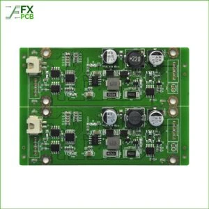
LED Light PCB Assembly refers to the process of mounting LEDs and other electronic components onto a printed circuit board (PCB) to create a fully functional LED-based device. These boards are the backbone of modern electronic lighting systems and are essential across multiple industries:
- Consumer electronics
- Automotive lighting systems
- Industrial and commercial lighting
- Medical-grade illumination solutions
- Smart home and IoT lighting devices
Choosing the Right LED Light PCB Assembly Manufacturer in China
Not all PCB manufacturers are equal. Choosing the right LED Light PCB Assembly Manufacturer is essential for optimal quality and performance. Here are the key things you should look for:
1. Evaluate the PCB Assembly Equipment
Efficient, high-speed, and accurate machines are critical for reliable production. A good manufacturer must have:
- High-speed pick-and-place machines
- Precision soldering stations
- Reflow ovens and wave soldering tools
Without reliable equipment, large-scale production of LED boards becomes difficult, and LED misplacement can impact performance and quality.
2. Confirm the Quality of LED Components
A PCB is only as good as its components. For lighting, LED quality is crucial. Top brands like Lumileds, Osram, Cree, Samsung, Luxeon, and Everlight (Taiwan) offer proven performance. Make sure your manufacturer sources LEDs based on your product’s purpose and environmental requirements.
3. Assess Their Assembly Process
Your chosen LED Light PCB Assembly Manufacturer should have a standardized and documented process that ensures consistency and reduces errors. At SFX PCB, we follow ISO9001 certified protocols for every production run, ensuring precision, accountability, and quality control.

Selecting the Right Materials for LED PCB Boards
Factors Determining Type of PCB Material
As a seasoned LED PCB Board Manufacturer, we know that material selection is critical. The right substrate impacts performance, durability, and thermal management. Here are the top considerations:
Fire Retardancy
Choose materials that slow down or suppress fire spread. Flame-retardant boards protect your end product and meet safety regulations.
Dielectric Constant
This indicates how well the material stores electrical energy—important for performance and compatibility in electrical circuits.
Dissipation Factor
Lower dielectric loss results in better electrical efficiency. High-quality laminates help reduce energy waste and heat buildup.
Tensile Strength
A good substrate won’t crack or stretch under pressure. Mechanical durability ensures longevity even in demanding environments.
Glass Transition Temperature (Tg)
Higher Tg materials withstand high operating temperatures without deforming making them ideal for heat-intensive LED applications.
Z-Axis Expansion
This defines how a material expands with heat. Materials with stable thermal coefficients resist warping and delamination.
Common Materials Used in PCB for LED Lights

CEM-1 and CEM-3
Cost-effective and flame-resistant, these are suitable for double-sided and multilayer PCBs. CEM-3 is often chosen for replacing FR4 in simpler LED applications.
FR4
A glass-reinforced epoxy laminate, FR4 is the industry standard. It offers excellent electrical insulation, mechanical strength, and heat resistance. It’s widely used for high-frequency circuits in PCB for LED lights.
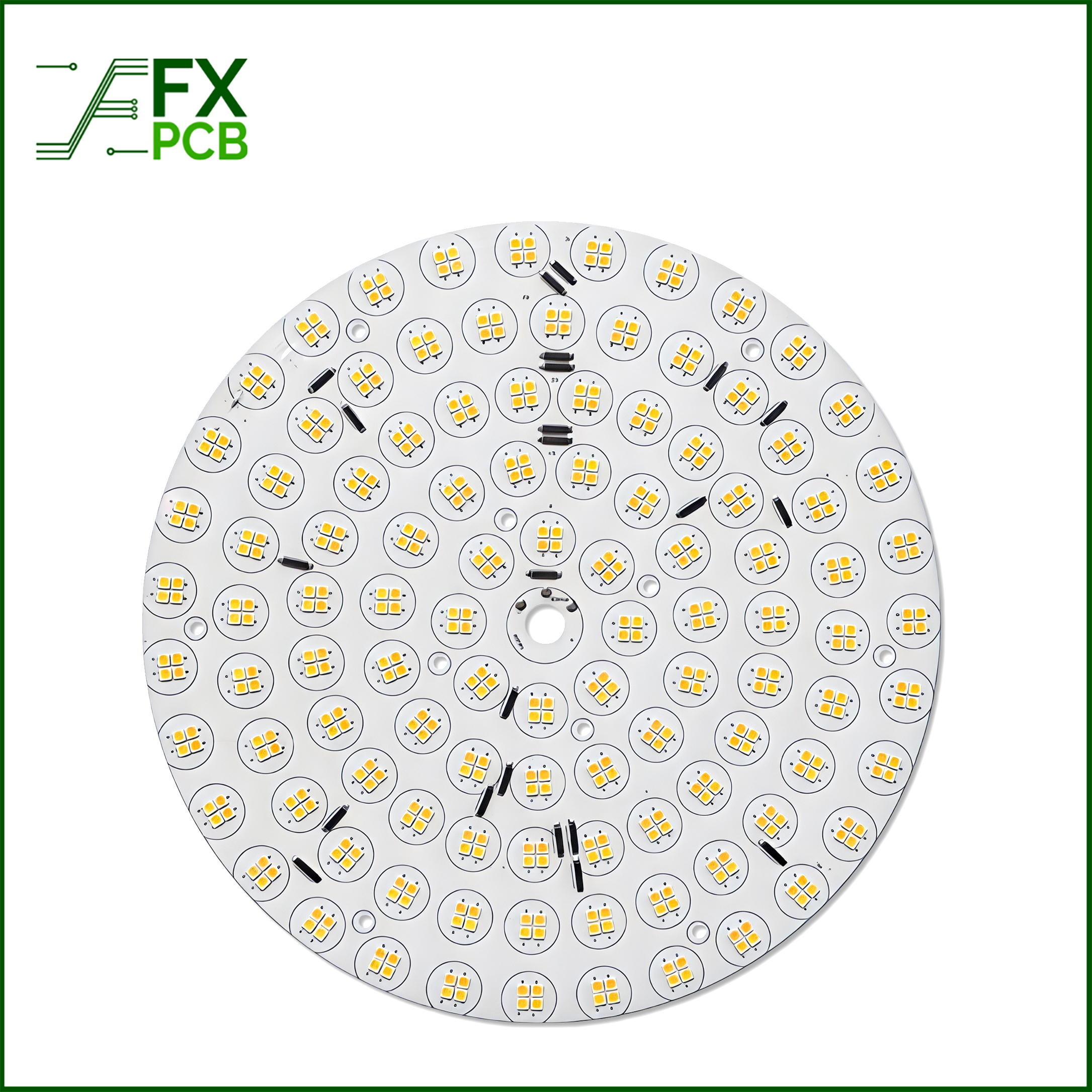
Aluminum
An industry favorite for thermal conductivity, aluminum core PCBs are ideal for high heat LED applications. They help dissipate heat away from LEDs improving life span and performance.
Copper Alloys
Used for their corrosion resistance and conductivity. Brass and bronze variants are durable and reliable in various environmental conditions.
Light PCB Manufacturing Process
Creating a high-performance LED PCB board involves several tightly controlled steps. Here’s how we do it at SFX PCB:
Step 1: Design and Output
Using software like Gerber, KiCad or Altium, we develop accurate design files that map out all PCB layers, pads and component placements.
Step 2: Design Review
Our engineers conduct a thorough design for manufacturability (DFM) review to catch any layout issues before fabrication.
Step 3: Printing the Circuit Layout
The design is transferred to a film or board via a plotter printer, which outlines the conductive and insulating sections.
Step 4: Substrate Fabrication
We prepare the substrate typically aluminum or FR4 by laminating, drilling and etching to define the circuit paths.

Step 5: Solder Mask and Silkscreen
The solder mask protects the board’s surface. While silkscreen labeling helps with component placement and identification.
Step 6: V Cutting and Routing
We separate individual PCBs from the panel using precise V cut or routing techniques without damaging board edges.
Step 7: Quality Checks and Testing
From electrical testing to visual inspections we ensure each LED Light PCB Assembly meets industry standards before moving to final assembly.
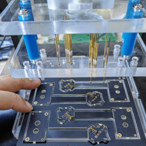
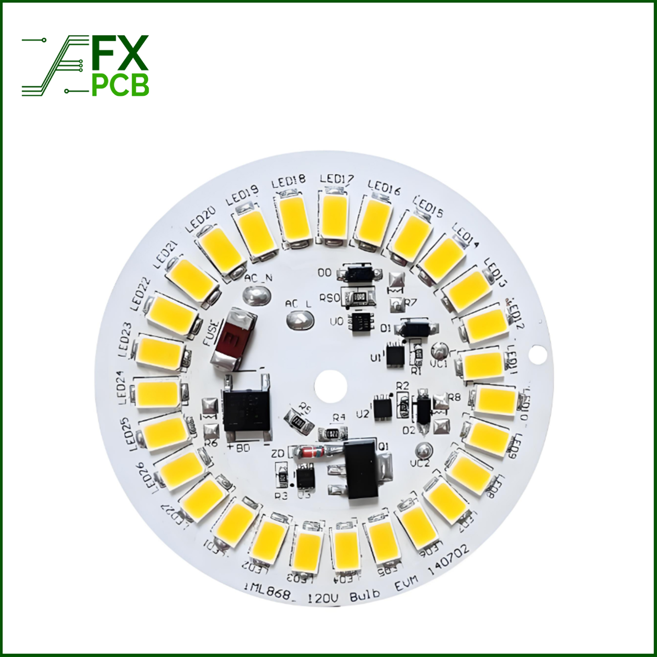
LED Light Circuit Board Assembly Process
At SFX PCB, we ensure your final LED PCB Board is not only functional but also durable. Here’s how our assembly process ensures quality:
Material Preparation
We carefully inspect every stencil, component, and bare board before the assembly begins. This includes checking your BOM and Gerber files.
Solder Paste Application
Solder paste is applied precisely using stencil printers to key points on the board.
SMT Component Mounting
Using our high-speed pick-and-place machines, SMT LEDs and components are accurately placed on the board.
Reflow Soldering
Boards are passed through a reflow oven, where controlled heating melts the solder and creates strong joints.
Through-Hole Component Insertion
If required, through-hole components are placed and soldered using wave soldering methods for extra strength.
Final Testing and Cleaning
We use AOI (automated optical inspection) tools to catch any issues before performing a final functional test. Clean boards are then packed with care and prepared for shipping.

Why Choose SFX PCB?
As a leading LED PCB Board Manufacturer in Shenzhen, we offer:
- 15+ years of industry expertise
- ISO9001 certified production processes
- Advanced machinery and inspection systems
- Flexible low to high volume order capacity
- Competitive pricing and fast turnaround times
Whether you’re making energy-saving home lights or powerful industrial floodlights, we’re the LED Light PCB Assembly Manufacturer trusted globally for reliability and new ideas.
Conclusion

Let’s create smarter lighting together. Contact us for a custom quote or learn how our LED PCBs can boost your next project. The manufacturing process for printed circuit boards (PCBs) is lengthy and complex and each step must be carefully carried out to guarantee the best possible performance of the finished board. Although the processes are repeated for a multilayered board, the fabrication process for single, double, and multilayered PCBs is essentially the same.
Shenzhen PCB assembly manufacturers like SFX PCB developed methods that enable the assembling of all LEDs. Shenzhen PCB assembly manufacturer is the ideal place for your Light PCB assembly needs. We can assist you in assembling everything from industrial high-power LEDs to commercial flood LEDs.