What is a PCB Stencil?
Friday, 06 October 2023
by FXSEO

What is a PCB Stencil?
In the dynamic world of electronics manufacturing, where the demand for smaller, more powerful devices is ever-increasing, precision is paramount. The production of modern printed circuit boards (PCBs) relies heavily on a critical tool that ensures accuracy in soldering – the PCB stencil. In this comprehensive guide, we will explore the intricacies of PCB stencils, their significance, various types, manufacturing processes, and how they contribute to the flawless assembly of electronic components.
Table of Contents
Our Recommended Quick Turn PCB

As a fast turnaround or quick-turn PCB Assembly Manufacturer /factory in Shenzhen China, FX PCB is able to fulfill orders in a fast delivery time with our modern technologies used in production.
Our factory carries out the assembly and installation of printed circuit boards to order. During the development and manufacturing process, constant quality control is carried out. We strictly follow your Gerber file and Bom list for your fast turnaround or quick turn PCBA projects, and we will also be glad to suggest you the alternative for your passive components to decrease your cost, but all replacement components need you to approve and make the final decision on whether you want to use them.
Understanding PCB Stencils
What is a PCB Stencil?
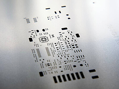
A PCB stencil, often referred to simply as an “SMT stencil,” is a thin sheet, typically made from stainless steel or polyimide, meticulously engineered with precise openings or apertures. These openings correspond to the locations of surface mount components on a printed circuit board. The primary purpose of a PCB stencil is to facilitate the precise application of solder paste during the PCB assembly process.
The Significance of PCB Stencils
1. Precision Solder Paste Application
The heart of the PCB stencil’s role lies in ensuring the precise deposition of solder paste onto the PCB. Solder paste, a critical element in soldering, acts as the intermediary between electronic components and the PCB. By restricting the application of solder paste to specific areas, PCB stencils create precise connections, reducing the risk of defects.
2. Consistency and Reliability
Manufactured with meticulous precision using advanced techniques like laser cutting or chemical etching, PCB stencils guarantee consistency throughout the assembly process. Consistent solder paste application leads to reliable solder joints, minimizing the chances of soldering defects such as insufficient or excessive solder.
3. Component Alignment
PCB stencils play a pivotal role in the accurate alignment of surface mount components on the PCB. The openings in the stencil guide the placement of these components, ensuring they are positioned with pinpoint accuracy for optimal electrical connectivity.
The PCB Stencil Printing Process
Stencil Preparation
Before initiating PCB assembly, meticulous preparation of the PCB stencil is necessary. This involves a thorough cleaning to remove any remnants of solder paste from previous uses and ensuring its precise alignment with the PCB.
Solder Paste Application
With the stencil firmly positioned over the PCB, solder paste is carefully applied onto the stencil’s surface. The precise locations for solder paste deposition are dictated by the openings in the stencil.
Squeegee Printing
A squeegee, typically composed of rubber or metal, is employed to uniformly spread the solder paste across the stencil. The squeegee’s motion pushes the paste through the stencil apertures, accurately depositing it onto the PCB.
Stencil Removal
Once the solder paste has been evenly applied, the stencil is gently lifted from the PCB. This leaves solder paste patterns on the PCB that precisely match the component pad locations.
Component Placement
Surface mount components are then meticulously positioned onto the PCB, guided by the solder paste. The paste acts as a temporary adhesive, temporarily securing the components in their designated positions.
Reflow Soldering
The fully assembled PCB, complete with components and solder paste, undergoes reflow soldering. During this stage, the assembly is subjected to specific temperature profiles, causing the solder paste to melt and form strong electrical connections between components and the PCB.
Inspection and Quality Control
Following reflow soldering, a thorough inspection is conducted to ensure proper soldering. Any defects or soldering issues are identified and rectified at this stage to ensure the final product’s quality and reliability.
Types of PCB Stencils
Framed Stencils
Framed stencils are the most common type of PCB stencils. They are characterized by a rigid frame that surrounds the stencil material. This frame provides stability and simplifies stencil alignment with the PCB.
Frameless Stencils
In contrast, frameless stencils lack a rigid frame. They are often used in automated stencil printers and are known for their cost-effectiveness and flexibility.
Step Stencils
Step stencils have varying thickness levels across the stencil, allowing for multiple solder paste deposits with varying heights. This proves advantageous in designs requiring different solder volumes for specific components.
The Role of PCB Stencils in Modern Electronics
As the electronics industry continues to push the boundaries of innovation, the demand for smaller, more intricate electronic devices grows. Mobile phones, laptops, tablets, and wearable technology all rely on the precision and efficiency that SMT technology, and by extension, PCB stencils, provide.
Conclusion
In the complex and ever-evolving world of electronics manufacturing, PCB stencils stand as unsung heroes. These unassuming sheets of material wield immense power by ensuring precise solder paste application, maintaining consistency, and guaranteeing the reliability of PCBA. As electronic devices continue to advance, the humble PCB stencil remains a cornerstone tool in the creation of our increasingly interconnected world. The next time you hold a sleek, high-tech gadget, you’ll appreciate the role that the unassuming PCB stencil played in its creation.

Peter Gong
I am Peter Gong. I have been working in PCB and PCBA industry for 15+ years now. I have been a part of the PCB revolution with my dedication to circuit board technologies and creative ideas. I write in FX PCB to impart my knowledge on PCB and PCBA for all circuit board lovers, manufacturers, and users.
Our Recommended Products for You


- Published in Informative
No Comments