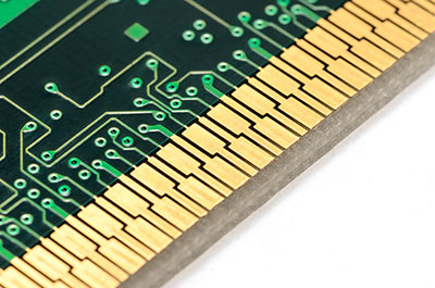
PCB Gold Fingers: What You Should Know
SFX PCB works with ceramic PCB and varieties of PCB products. So, we have decided to share the definition and its uses with our readers. Ceramic PCB is a circuit board made with a ceramic base material.
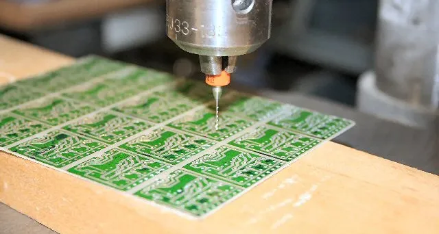
PCB Drilling – The Detailed Discussion
SFX PCB works with ceramic PCB and varieties of PCB products. So, we have decided to share the definition and its uses with our readers. Ceramic PCB is a circuit board made with a ceramic base material.
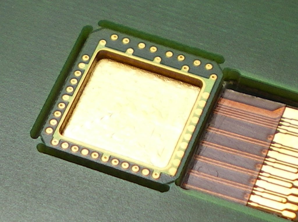
What Is Cavity PCB: Advantages, Applications, and Manufacturing
SFX PCB works with ceramic PCB and varieties of PCB products. So, we have decided to share the definition and its uses with our readers. Ceramic PCB is a circuit board made with a ceramic base material.
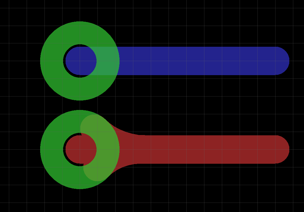
PCB Teardrop: Importance, Design, and Manufacturing
SFX PCB works with ceramic PCB and varieties of PCB products. So, we have decided to share the definition and its uses with our readers. Ceramic PCB is a circuit board made with a ceramic base material.
What is a PCB Stencil?
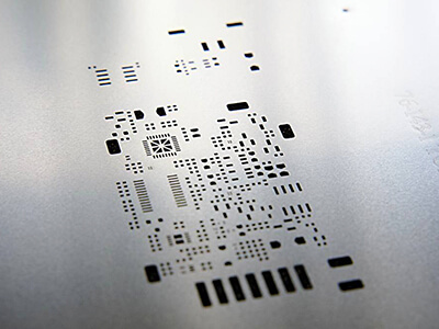
SFX PCB works with ceramic PCB and varieties of PCB products. So, we have decided to share the definition and its uses with our readers. Ceramic PCB is a circuit board made with a ceramic base material.
Protoboard vs. Breadboard
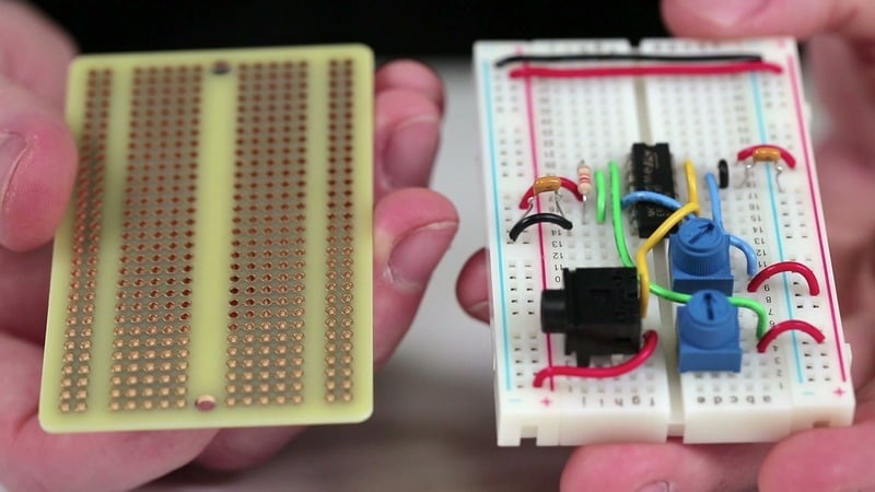
SFX PCB works with ceramic PCB and varieties of PCB products. So, we have decided to share the definition and its uses with our readers. Ceramic PCB is a circuit board made with a ceramic base material.
How to Use a Breadboard and How It Works
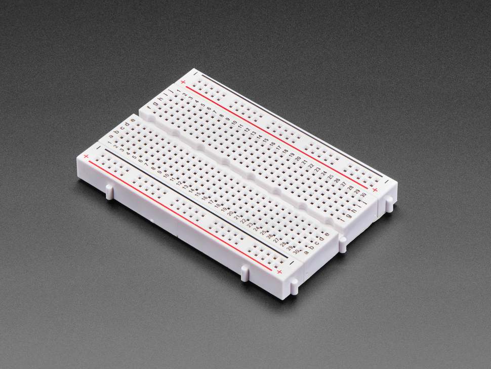
SFX PCB works with ceramic PCB and varieties of PCB products. So, we have decided to share the definition and its uses with our readers. Ceramic PCB is a circuit board made with a ceramic base material.
PCB HS Code Complete Guide
SFX PCB works with ceramic PCB and varieties of PCB products. So, we have decided to share the definition and its uses with our readers. Ceramic PCB is a circuit board made with a ceramic base material.
Significance of Quick Turn PCB for Modern Electronics
SFX PCB works with ceramic PCB and varieties of PCB products. So, we have decided to share the definition and its uses with our readers. Ceramic PCB is a circuit board made with a ceramic base material.
BGA PCB (Ball Grid Array Printed Circuit Boards)
SFX PCB works with ceramic PCB and varieties of PCB products. So, we have decided to share the definition and its uses with our readers. Ceramic PCB is a circuit board made with a ceramic base material.