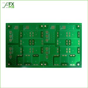
Description
Why Choose an 8-Layer PCB?
When designing the PCB, you may find that 4 or 6 layers are not enough. Our 8-Layer PCBs are the ideal solution, as it has two additional signal layers than 6-layer PCBs to optimize the arrangement of power and ground planes, thus they can reduce the potential for electromagnetic interference and crosstalk.
Our capability for 8 Layer PCB:
| Layers | 8 Layers |
| Material | FR-4, Rogers, High Tg |
| Max. Board Size | 450x800mm |
| Min. Trace/Space | 3/3 mil (0.075/0.075 mm) |
| Min. Drill Size | 6 mil (0.15 mm) Mechanical / 4 mil (0.10 mm) Laser |
| Finished Copper Weight | 0.5 oz – 1oz (Inner/Outer) based on 3/3 mil trace/space 0.5oz-10oz based on normal trace/space width |
| Through-Hole Plating | Cu 20 µm (0.8 mil) min |
| Solder Mask | Green, Red, Blue, Black, White, Yellow |
| Surface Finishes | ENIG, HAL Leadfree, Immersion Silver, HASL, ENEPIG, OSP, Immersion Tin, Hard gold plating, Soft gold plating |
| Impedance Control | ±10% tolerance |
| Others | Blind&Buried Vias, Microvias, edge plating, Gold Fingers |
Comparison of Different 8 Layer stack-up
The different stacking of an 8 Layer PCB will affect the PCB cost, performance, and manufacturability. Here is the normal stack-up that an 8 Layer PCB will usually use
| Layer No | Stackup 1 | Stackup 2 | Stackup 3 |
| Top | Signal | Signal | Signal |
| 2 Layer | GND1 | GND1 | GND1 |
| 3 Layer | Signal | Signal | Signal |
| 4 Layer | GND2 | PWR | Signal |
| 5 Layer | PWR | GND | PWR |
| 6 Layer | SIgnal | SIgnal | SIgnal |
| 7 Layer | GND3 | PWR | GND |
| 8 Layer | Signal | Signal | Signal |
Stackup Option 1: This stackup is currently the industry-recommended 8-layer PCB configuration, comprising 4 signal layers, 1 power plane, and 3 ground planes. The layer structure delivers optimal signal integrity, power integrity, and EMC performance. Layer 3, adjacent to two ground planes, provides the optimal routing environment—prioritize high-speed and sensitive signals on this layer. The spacing between Layer 4 and Layer 5 should be minimized to achieve lower plane impedance for the power plane on Layer 5. Both Layer 2 and Layer 7 are ground planes and may serve as return paths for high-speed signals.
Stackup Option 2: TOP, GND02, S03, PWR1_04, GND05, S06, PWR2_07, BOTTOM
This stackup is suitable for designs with multiple power types. Layers 3 and 6 are the optimal routing layers. The spacing between Layer 4 and Layer 5 should be reduced to lower the impedance of the PWR2 plane. Signal routing on Layer 8 should be minimized, with large-area copper pours applied appropriately on Layer 8 to reference the Layer 7 plane. To maintain PCB stackup symmetry, appropriate copper pouring should also be applied on the TOP layer.
Stackup Option 3: TOP, GND1_02, S03, S04, PWR05, S06, GND2_07, BOTTOM
This stackup provides 5 routing layers, 1 power plane, and 2 ground planes. It offers poor power integrity and decoupling performance and is generally used in cost-sensitive designs requiring more routing layers, such as consumer tablets. Layers 3 and 6 are preferable for routing. The spacing between Layer 3 and Layer 4 should be increased during design, and signals on these layers should be routed orthogonally to minimize interference.
Why You choose FX PCB as your supplier?

You’ve Got Questions. We’ve Got Straight Answers.
Q: My design is on a 6-layer board. When should I consider moving to 8 layers?
A: Usually for two reasons: First, if you’re struggling with routing congestion and the design is a mess. Second, and more importantly, if you’re seeing signal integrity or power delivery issues in testing. The two extra layers give you the room and the shielding to fix it.
Q: Can you recommend me an 8 Layer PCB stack-up based on my design?
A: Yes, Send us your requirements, and our engineers will recommend a layer stack-up that optimizes for your signal speed, impedance control, and EMI needs.
Ready to See the Difference 8 Layers Can Make?
You could choose any PCB supplier. But if you need a board that performs as hard as you do, you need a partner who understands the engineering behind it.
Upload your Gerber files for a quote. and our engineer will review your design and provide a real-person DFM analysis. We’ll point out potential issues before they become costly problems.
Get your quote and design review now. Let’s build something reliable together.