Description
OSP Printed Circuit Boards Manufacturer
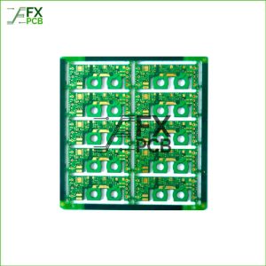
As a Manufacturer of PCB boards in China, FX PCB can produce OSP Printed circuit boards, ENIG PCB, HAL Leadfree boards and etc. We will introduce you to the OSP PCB boards below:
OSP, “organic solderability preservatives,” is a bare finish on the copper foil to prevent it from oxidation. Its use in PCB surface finish is increasing fast due to its eco-friendliness, cost-effectiveness, and longevity. It preserves the copper from oxidation for use in later parts of PCB manufacturing through soldering.
Hence, OSP printed circuit board manufacturers use it to enhance the endurance and longevity of their PCBs. The water-based organic coating ensures copper is not oxidized and stays in good condition. It improves the storage time and makes the copper foil and PCB reworkable.
Knowing about OSP and its integration with PCB will be valuable if you are in the PCB manufacturing or appliance-making sector. Following it, we will show you the details of OSP, its benefits, and ways to use it. We will discuss different PCB Surface finish types in today’s article. So, stay with us to know these intriguing details and find the perfect PCB finish.
What Is OSP Process?
OSP, or organic solderability preservatives, is a layer of compound organic finish on the bare copper foil. It sits over the copper surface through the adsorption process. It is also referred to as anti-tarnish because it preserves the copper surface from tarnishing due to oxidation.
OSP manufacturing brings two immediate features to copper-based PCBs. These are:
- The OSP finish on the copper layer protects it from moisture, thermal shock, and oxidation. So, it prolongs the lifespan of the bare copper surface until it is used in PCB engineering.
- During the soldering process, OSP finish can be fluxed easily for using copper in PCBs. It enhances the shelf life of the copper layers for the best applications in printed circuit boards.
OSP coating PCB uses an organic compound chemical on the copper surface. It comes from the “Azole family” and perfectly sticks to the copper surface. Also, the organic compound is water-based. So, it is easily soluble and removable from the surface whenever required.
The compound reacts with the copper atom and bonds when applied on the surface to create a thin covering. Thus, it forms a film over the copper and safeguards it from coming in touch with the air. So, the elements in the air won’t react with the copper. This way, the surface stays in good condition without any oxidation.
The thickness of the compound film on the surface depends on the compound the PCB manufacturer uses. Usually, OSP PCB finish manufacturer will use benzotriazoles, imidazoles, and benzimidazoles. These chemicals dissolve on the surface to create a filmy cover.
- Benzotriazole surfaces form a thinner film on the copper foil
- Imidazole surface forms a thicker film for better preservation
Of course, the thickness of the film directly controls the performance of the PCB-finished products. It also depends on the OSP PCB manufacturing process.
OSP PCB Manufacturing Process:
The OSP integration on the printed circuit board surface goes through multiple rising with water and deionization processes. After multiple rinsing with water, acid, and DI (Deionization material), the OSP is applied on the PCB bare surface. Then, it is dried and stored for circuit board integration.
The manufacturing process includes:
![]()
The cleaning process aims to remove the impurities from the copper surface using water, acid-based, and DI cleaning materials. It removes the following materials from the copper surface:
- Oil
- Oxidation layer
- Fingerprints
- Any impurities
Through multiple cleaning and rinsing processes, it makes the copper surface pure. Finally, manufacturers will apply the OSP on the bare and cleaned surface. So, it forms the filmy layer and stops the copper from coming in touch with the external elements.
Plus, manufacturers will apply high-end micro-etching over the surface during the topography enhancement. It removes any traces of oxidation from the copper foil and makes it as clean as possible. So, it helps in better bonding between the OSP application and copper foil. As the cleaning and topography enhancement processes are essential, manufacturers will inspect them regularly.
The film development rate on the copper depends mainly on the micro-etching speed. So, PCB manufacturers will control the etching speed for an even smooth coating on the copper foil. The standard micro-etching speed is 1.0 to 1.5μm every minute.
After the topography enhancement process, the surface goes through acid rinsing again. This step uses 5% to 15% sulphuric acid to rinse the copper foil. So, it removes maximum traces of oxidation and impurities from the copper.
Then, manufacturers will apply the compound chemicals from the “Azole family” to form the OSP coating PCB finish. As soon as OSP coating starts forming, they will apply DI (Deionization) material to remove other ions from the OSP application. So, there will be only the “Azole family” compound and copper ions. They will bond and form the anti-tarnishing layer.
For DI rinsing after preservative development, choose a cleaner with pH5 to pH7. If the cleaner is too acidic, it will remove the OSP preservation from the copper foil. As a result, the entire process will become useless, and you will have to start it again.
Why USE OSP
The conventional SMT (Surface Mounting Technology) will use the bare copper surface for PCB manufacturing. So, why should you choose an OSP PCB surface finish? What benefits does it bring to you? Well, it will enhance the lifespan of bare PCBs. Plus, it improves the thermal shock-absorbing ability of the surface. As a result, it can work in extreme conditions.
Easy fabrication:
OSP application keeps the copper surface fresh and undamaged. So, when engineers start the PCB fabrication, they will find the copper layer uncontaminated and in good condition. As it remains free from oxidation, soldering gets easier. Also, it helps better bond the copper layer with the substrate and other integrations on the base.
Improves wettability:
PCB requires maximum wettability for proper soldering. Regarding this, the OSP application improves the wettability of the PCBs superbly. As the flux meets the pads and vias during the soldering process, its improved wettability provides a better finish.
Cost-friendly:
OSP finish on PCB uses simple and organic chemical compounds. These are cost-effective and easily gettable. So, it keeps the PCB manufacturing cost reasonably low. Moreover, it saves the copper layer from damage and improves the user ratio. PCB manufacturers will see a considerable cost reduction in their soldering and circuit board manufacturing.
Double-sided SMT:
OSP now enables PCB manufacturers for double-sided SMT assembly. Previously, it had only single-sided SMT assembling. Now, with double-sided SMT assembly, OSP-printed circuit boards are used widely in different sectors.
Eco-friendly:
OSP applications use water-based compounds. So, it is easily disintegrated and won’t harm the environment. As a result, OSP PCBs are known for their eco-friendly attributes. It won’t damage the environment while OSP integration.
Also, removing the OSP coating from the copper quickly dilutes it in water without adding extra chemicals and additives. It becomes more accessible for PCB manufacturers to maintain industry standards and compliance accurately.
As you see, OSP printed circuit board manufacturers have better improvements than regular ones. And SFX PCB follows strict guidelines in manufacturing the most-splendid OSP PCBs for you following industry guidelines.

The diagram shows the benefits of using OSP-printed circuit boards. However, the PCB surface finish may be done in other ways too. Let’s look at the top surface finish types you can choose for PCBs.
PCB Surface Finish Types:
PCB manufacturers use different types of surface finishes for their printed circuit boards. All these surface finishes bring their benefits.
ENIG finish PCB:
ENIG, or Electroless Nickel Immersion, is the most widespread PCB surface finish these days. The metallic coating has a double layer, and nickel is the main component of it. Firstly, nickel acts as the substrate for soldering the PCB components. Secondly, the nickel coating also works as a copper barrier to protect it from damage.
There’s also a thin layer of gold over the nickel. It saves the nickel from scratches during storage. You will see ENIG finish PCBs mostly in lead-free industries. So, appliances and devices that won’t use lead-based PCB finishing will apply ENIG.
Although it improves the stability and strength of the substrate and copper surface, there’s a downside. Often the phosphorus will develop between the gold and nickel layers. It could damage the circuit board shortly.
Pros:
- Improves strength and stability
- Flat surface good for PTH
- Requires no lead at all
Cons:
- Expensive processing
- It doesn’t suit reworking
HASL PCB Finish:
HASL is one of the oldest and most-affordable surface finishes for PCBs. It uses a lead or tin melting pot. Then the PCBs will be immersed in this melting pot. Then, manufacturers will use an air knife to remove the excess soldering materials and solders from the circuit board.
HASL exposes the soldered PCBs up to 265°F temperature. It quickly highlights the potential delamination on the circuit board. So, manufacturers may quickly observe any expensive materials attached to the PCBs. Once they find these materials, they can remove them. What’s more, the HASL surface finish is affordable and supports easy soldering.
However, with time, PCB manufacturers have realized its faults. It makes the PCB surface uneven. Also, it’s not suitable for fine-tuning and high-end devices.
Pros:
- Easy to repair
- Widely available
- Low-cost finish
Cons:
- Uneven surface
- Poor wettability
- Prone to thermal shocks
HAL Lead-free PCB finish:
The HAL lead-free PCB is similar to the HSAL surface finish. The difference is that it doesn’t use any lead for purifying the PCBs. Like the HASL surface finish, it is also low-cost. So, manufacturers have been choosing the lead-free HAL surface finish to save money.
What’s more, lead-free HAL approves quicker finish. It also operates at up to 265-degree temperatures. So, it exposes the defects and accuracy in the printed circuit boards better. Also, with exposure, manufacturers can quickly identify the expensive objects attached to the PCB substrate. It allows them to remove the impurities and work with the purest PCBs.
Pros:
- Allows reworking facility
- Most-affordable surface finish
- Lead-free finish for better uses
Cons:
- Low endurance
- Solder bridges soon
ENEPIG PCB finish
ENEPIG is one of the most advanced PCB surface finishes. It includes three layers:
- At first, there will be electroless nickel 150-200 micro-inch thick.
- Secondly, an 8-15 micro-inch thick electroless palladium layer.
- Thirdly, there will be a gold layer with 1 to 2 micro-inches thickness.
ENEPIG, with its three layers of protection, is superior to the standard ENIG finish. It suits all types of wire bonding, unlike the ENIG surface finish. Also, you will see its uses widely in soldering. So, it suits regular soldering and wire bonding for the printed circuit boards.
While ENIG finish suffers from the “Black-pad” consequence, ENEPIG finish is free from it. So, manufacturers choose it for better longevity and strength. Its application is identical to the ENIG surface finish. Its widespread use and benefits have earned it the name “Universal Surface Finish.”
Pros:
- Gold and aluminum wire bonding
- Brilliant soldering capacity and strength
- Decreased price of palladium
- Quick and easy surface application
Cons:
- It needs multiple metals for finish and so is time-consuming.
Immersion Silver PCB finish:
If the printed circuit manufacturer looks for flat pack coating and fine pitch, an immersion silver PCB finish is perfect. In fact, this surface finish contains OSP PCB surface finishing, which makes it anti-tarnishing. Thus, it enjoys greater stability and strength.
Also, the combination of OSP and immersion silver for the surface finishing enhances its shelf life. It has a moderate shelf life of up to 12 months. So, after preparing the PCB, it can sit back for a long time. When you work with the PCB, its copper foil will remain intact.
Pros:
- RoHS complaint
- Cost-effective finish
- Stable and rugged
- Ideal for fine pitch
Cons:
- Compliant-pin intervention (Ni-Au Pins) needs to be improved.
Conclusion
OSP printed circuit board manufacturers choose it for stability, strength, and longer shelf life. Its anti-tarnishing feature will help the circuit board remain in good condition. So, the copper foil survives oxidation and serves better in the harshest conditions. Following it, SFX PCB has adapted the latest OSP PCB surface finishes for more intricate home appliances and devices. If you need a superior finish of the PCB for use at industrial levels, FX PCB-made OSP printed circuit boards will be your choice. We provide customized orders cost-effectively and will deliver the circuit boards faster. Our streamlined manufacturing and shipment enable us to quickly meet your high-quality OSP PCB demands.