When you 1st start developing your device, you may need to shift wiring and component set up frequently before you find the fine-tuning. The printed circuit board with its rigidity and flexibility will allow you these component substitutions and wire shifting thanks to its highly customizable design.
Here, we will discuss the ins and outs of a custom PCB board, so you know how to get your perfectly customized printed circuit board. Also, we will show how you can cut down the cost of manufacturing printed circuit boards without compromising the quality.
Furthermore, we will show the techniques to manufacture custom circuit boards easily for DIY and hobbyists for some easy-going projects.
You must understand that when you have the flexibility to translate the one-off circuit board project into a fully tailored PCB design, you may develop different device designs on it easily. Therefore, you will see how custom boards help you in multiple ways from cost-cutting to avoid technical difficulties.
First off, let’s clarify the definition of the PCB or printed circuit board. It consists of an insulating layer that is thick and rigid. You will find the conductive traces both on the upper and lower side of the insulating layer.
The insulating layer stops the malfunctioning of different electrical and electronics components on both sides for superior performance. Also, you connect the conductive traces on both sides via holes, if need be. So, PCBs come with easy flexibility and rigidity to develop any device using their unique diagram.
You can customize the PCB design to prepare your circuit design and PCB Assembly to work on them for your devices. The benefits of custom PCB are that you can choose the material of the insulating layer and order for the tailored conductive traces that meets your project requirements.
As a hobbyist, manufacturing your 1st printed circuit board isn’t going to be easy. It will need several trial and error tries and only then, you will be able to truly get your customized circuit boards.
First off, you will need to layout the required PCB in its schematic view. You will need a canvas for it on which you will put all the necessary components. The components will come from mainly a component library. It is included within the software design to build the custom circuit boards.
When you layout the components on the canvas, you will have to draw lines between the pins. It will represent the connections. The good thing is that for each part number of the components you have the freedom to choose from multiple options for arrangement.
The ability to choose from different components and parts numbers mainly come from the fact that these components come in various packages. The most common of them is the Dual In-Line Packaging (DIP) and System In-Line Packaging (SIP). Hobbyists will always prefer the SIP and DIP over the single-line packaging although these are usually chunky and a little bit expensive.
Also, DIY workers and hobbyists choose DIP and SIP components because these are easily found in hardware shops. Furthermore, these components are easier to handle than the surface mount components. The surface mount components are used mostly for commercial purposes and also, need a higher degree of skills for handling them properly.
When your layout is ready, it’s time to move to the next step. At this time you may want to add the required ground or power signals along with the connections. But it is not always necessary.
FX PCB has a big component library that allows the manufacturer to arrange these interconnections and component setups better. Also, you may get the custom printed circuit boards readily available from us if you don’t want to build them.
Anyways, when your layout is entirely ready ensuring that everything is placed right where it needs to be, you need to check the setup. This is known as Electrical Rule Change (ERC) The ERC will highlight the common glaring problems of the PCB setup including wire connections.
You may switch to the other side of the PCB layout once you are satisfied that the circuit board has no errors in connection and design. You will see that the components on the board are arranged randomly instead of any systematic orders. As the wires aren’t connected with the pins, you need to move the components safely to arrange them.
When the layout design is completed on both sides, you can give the printed circuit board a final check. It is known as the Design Rule Check (DRC). You can upload the custom circuit board design and start working on it practically once it passes the DRC checking successfully.
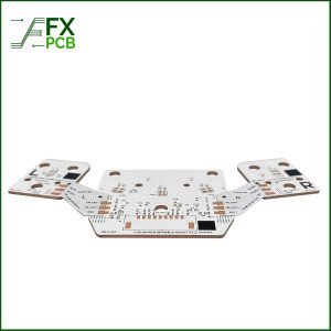
The top is covered with silk-screen lettering. It allows the device manufacturer to quickly identify the number of the different parts and which component is placed where.

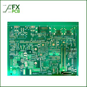
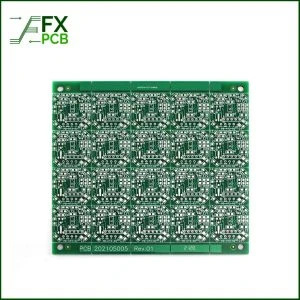
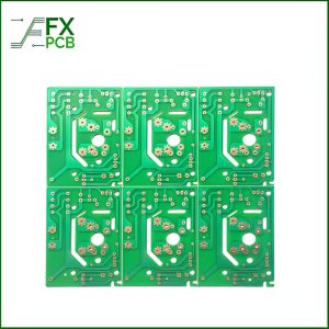
FX PCB excels in printed circuit board designing for the past 10+ years. We have experience in making aluminum, ceramic, flex, rigid, and rigid-flex PCBs of all sorts. Our design layout comprises from the simple one to the most complex that fulfills the needs of both hobbyists and professionals.
Also, we permit you to find the right-sized printed circuit board that fulfills your necessity unlike forcing you to choose from our preplanned designs. Our flexible offerings with competitive pricing enable you to choose your right circuit board with the best customization.
Last but not least, whether you need bulk orders for the custom circuit boards or only a few hundreds of prototypes, we deliver them all in the shortest possible time. So, you won’t have to bargain to get your needed numbers of PCBs.
Custom PCB boards offer you to build various devices easily and quickly. If you are unsure about your circuit board skill, you can always get the PCBs from a reputed manufacturer such as FX PCB. You will love how these customized printed circuit boards bring flexibility and freedom to your circuit board applications for greater applications.

I am Peter Gong. I have been working in PCB and PCBA industry for 15+ years now. I have been a part of the PCB revolution with my dedication to circuit board technologies and creative ideas. I write in FX PCB to impart my knowledge on PCB and PCBA for all circuit board lovers, manufacturers, and users.
WhatsApp us