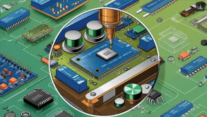
Before choosing the right 6-layer PCB manufacturer in 2025, let FX PCB introduce you the benefits of 6-layer PCBs.
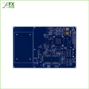
What is a 6-Layer PCB?
A 6-layer PCB is designed with alternating layers of copper and insulation, enabling the integration of complex circuits for advanced electronics such as telecommunications, aerospace, and consumer devices. By incorporating signal, ground, and power planes, it reduces noise, improves signal integrity, and enhances thermal management. This makes it an ideal choice for high-frequency, high-speed, compact, and performance-driven applications.
Why Choose a 6-Layer PCB?
A 6-layer PCB offers unmistakable focal points over less difficult plans, making it the favored choice for engineers and producers working on complex and high-performance applications. Here’s why:
- Compact Plan: With six layers, you’ll be able coordinated more circuitry into a littler physical impression, culminate for compact and versatile gadgets.
- Progressed Flag Judgment: Committed ground and control planes minimize cross-talk and impedances, guaranteeing dependable flag transmission.
- Higher Thickness: The multi-layer arrangement bolsters complex flag steering, basic for progressed and perplexing plans.
- Decreased Electromagnetic Obstructions (EMI): Key layer stacking altogether diminishes EMI, moving forward generally execution in touchy frameworks.
- Warm Administration: The extra layers help in viable warm scattering, basic for high-power and high-speed applications.
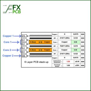
Point by point Structure of a 6-Layer PCB
A 6-layer PCB comprises of six stacked layers, each fastidiously outlined to fulfill a particular part. This layered structure empowers effective flag directing, control dispersion, and warm administration. Here’s a point by point breakdown of its structure:
Layer 1: Beat Flag Layer
- This is often the essential layer utilized for surface-mounted components, follows, and external associations.
- It acts as the most interface for components like ICs, resistors, and capacitors.
Layer 2: Ground Plane
- The ground plane is devoted to giving a steady reference point for signals.
- It minimizes clamor, decreases electromagnetic obstructions (EMI), and moves forward generally flag judgment.
Layer 3: Internal Flag Layer
- This layer is outlined for directing perplexing signals that cannot fit on the external layers.
- It is especially compelling for overseeing high-speed and high-frequency flag pathways.
Layer 4: Control Plane
- A devoted layer for control dispersion, guaranteeing steady voltage conveyance over the board.
- It decreases control commotion and makes a difference optimize the execution of power-sensitive components.
Layer 5: Inward Flag Layer
- Comparative to Layer 3, this layer gives extra directing space for thick circuits.
- It is particularly valuable in complex plans where different flag ways have to be overseen.
Layer 6: Foot Flag Layer
- The foot layer is regularly used for soldering, extra follows, or outside associations.
- Just like the top layer, it serves as an interface for components and upgrades plan adaptability.
6-Layer PCB vs. Other PCBs
To way better get it the points of interest of 6-layer PCBs, let’s compare them with other sorts of PCBs:
| Aspect | Single-Layer PCB | 6-Layer PCB |
| Layers | 1 conductive layer | 6 conductive layers |
| Complexity | Simple | Highly complex |
| Applications | Basic devices (e.g., remotes) | High-speed, advanced devices |
| Cost | Low | Relatively higher |
Multilayer PCBs (4-Layer vs. 6-Layer)
| Aspect | 4-Layer PCB | 6-Layer PCB |
| Layers | 4 conductive layers | 6 conductive layers |
| Performance | Good for moderate speeds | Excellent for high-speed circuits |
| Heat Management | Limited | Better due to additional planes |
How Are 6-Layer PCBs Fabricated?
Fabricating a 6-layer PCB requires accuracy, progressed strategies, and thorough quality control to meet the requests of high-performance applications. Here’s a nitty gritty step-by-step breakdown:
- Plan and Format
- Engineers utilize specialized computer program like Altium Originator, Hawk, or KiCad to make the PCB format.
- This arrange incorporates characterizing the stack-up arrangement, flag ways, and component situation to guarantee ideal execution and negligible impedances.
- Fabric Determination
- High-quality materials like FR4, Rogers, or Teflon are chosen based on the application’s necessities, such as warm solidness, flag execution, and natural solidness.
- The choice of materials altogether influences the PCB’s unwavering quality and execution.
3.Layer Stacking
- The six layers, comprising of substituting conductive copper and insulating dielectric materials, are stacked within the adjust arrange.
- Legitimate arrangement amid this prepare is basic to guarantee that flag ways and associations work as planning.
- Boring
- Gaps for vias (connections between layers) are penetrated utilizing CNC machines to attain exact and precise situations.
- This step empowers consistent electrical network over all layers.
- Plating
- Copper plating is connected to the penetrated gaps, making conductive pathways between layers.
- Electroplating guarantees uniform scope and conductivity.
- Carving
- Undesirable copper is evacuated from the layers to create circuit designs.
- Methods like chemical or laser carving are utilized to form intricate and exact pathways for signals.
- Cover
- The stacked layers are reinforced together beneath tall warm and weight in a laminating machine.
- This step comes about in a bound together, tough PCB structure.
- Patch Veil Application
- A defensive patch cover is connected to the board’s surface to anticipate oxidation and coincidental brief circuits.
- This layer moreover gives the PCB its characteristic green (or other) color.
- Silkscreen Printing
- Names, images, and identifiers are printed on the board for less demanding component arrangement, gathering, and investigating.
- Quality Testing
The wrapped up PCB experiences thorough testing to guarantee usefulness and unwavering quality, counting:
- Electrical testing to confirm network.
- Impedance testing for high-frequency applications.
- Warm testing to assess warm resilience and solidness.
Benefits and Applications of a 6-Layer PCB
A 6-layer PCB could be a exceedingly flexible and progressed circuit board that gives unmistakable focal points over less difficult plans, making it an fundamental choice for engineers and producers working on high-performance applications. Underneath, we dive into its benefits and differing applications.
Benefits of a 6-Layer PCB
- Upgraded Flag Judgment
- One of the standout benefits of a 6-layer PCB is its predominant flag judgment. Committed ground and control planes minimize obstructions, cross-talk, and flag misfortune, guaranteeing steady and dependable execution.
- This highlight is especially vital in high-speed and high-frequency applications, where indeed minor obstructions can disturb operations.
- Higher Circuit Thickness
- With six layers, these PCBs offer more directing alternatives, permitting engineers to coordinated complex circuitry into a compact plan.
- This makes 6-layer PCBs perfect for applications where space is constrained, however execution requests are tall.
- Made strides Warm Administration
- The multi-layer structure successfully disperses warm over the board, anticipating overheating and dragging out component life.
- This advantage is basic in applications requiring ceaseless operation beneath tall control loads.
- Versatility
- 6-layer PCBs are outlined to suit high-speed and high-frequency circuits, making them adaptable for future overhauls and developments.
- Their capacity to bolster complex flag steering ensures adaptability to advancing innovations.
- Clamor Decrease
- Appropriate layer stacking in a 6-layer PCB minimizes electromagnetic obstructions (EMI), diminishing clamor and moving forward by and large execution.
- This makes them appropriate for touchy applications where flag clarity is basic.
Applications of 6-Layer PCBs
Due to their progressed highlights, 6-layer PCBs are utilized over a wide extend of businesses, counting:
- TBroadcast communications
- Gadgets: Switches, switches, servers, and organizing hardware.
- Part: Guarantees quick information transmission, moo idleness, and solid network in basic communication frameworks.
- Aviation and Defense
- Gadgets: Route frameworks, aeronautics, radar frameworks, and partisan communications.
- Part: Conveys tall unwavering quality, exactness, and toughness in extraordinary situations.
- Therapeutic Gadgets
- Gadgets: Demonstrative gear, quiet screens, imaging frameworks, and convenient gadgets.
- Part: Offers compact plan, unwavering quality, and precision, which are vital in life-saving hardware.
- Customer Gadgets
- Gadgets: Smartphones, tablets, tablets, wearables, and gaming gadgets.
- Part: Gives the compact plan and tall execution required for convenient and multifunctional gadgets.
- Car
- Gadgets: Progressed Driver-Assistance Frameworks (ADAS), infotainment frameworks, motor control units (ECUs), and sensors.
- Part: Upgrades security, usefulness, and network in present day vehicles.
How to Select the Correct 6-Layer PCB Producer
Choosing the correct producer for a 6-layer PCB is basic for guaranteeing the victory of your extend. A well-qualified producer not as it were conveys high-quality PCBs but too ensures a smooth improvement handle and reliable conclusion items. Below could be a point by point direct to assist you make the correct choice, along side an diagram of key highlights, challenges, and future patterns in 6-layer PCB fabricating.
Components to Consider When Selecting a Producer
- Encounter and Ability
- Take producers with broad involvement in creating 6-layer PCBs for different businesses. A demonstrated track record illustrates their capacity to meet complex plan and execution necessities.
- Inquire about client surveys, case considers, and tributes to assess their capabilities. Explore for producers who specialize in high-frequency and high-speed plans, as these frequently require progressed procedures and exactness.
- Quality Guidelines
- Guarantee that the producer complies with industry certifications such as IPC (Organized for Printed Circuits), ISO (Worldwide Organization for Standardization), or UL (Guarantors Research facilities). These certifications reflect adherence to thorough quality measures.
- Affirm that the producer takes after rigid quality control forms, counting electrical and warm testing, to ensure unwavering quality.
- Prototyping Capabilities
- Prototyping is an fundamental step in PCB improvement. A producer with strong prototyping capabilities can rapidly create test forms of your plan, permitting you to approve and refine the PCB some time recently moving to mass generation.
- Speedy prototyping quickens the advancement handle and makes a difference distinguish potential plan blemishes early.
- Progressed Hardware
Cutting-edge apparatus is basic for fabricating exact and dependable 6-layer PCBs. Inquire producers almost their hardware and capabilities, such as:
- Impedance control for high-frequency plans.
- Laser boring for microvias.
- Programmed optical assessment (AOI) for quality checks.
- Fetched and Turnaround Time
- Whereas fetched is an critical figure, maintain a strategic distance from compromising on quality to spare cash. High-quality PCBs often result in superior execution and lower long-term costs due to diminished disappointments.
- Assess the manufacturer’s lead times to guarantee they can meet your venture due dates. Quick turnaround times are especially basic in businesses with tight plans.
6.Client Bolster
- Responsive and learned client bolster can altogether streamline the fabricating handle. Guarantee the producer gives help at each organize, from plan and prototyping to generation and conveyance.
- A committed account chief or back group can make communication more compelling and address issues expeditiously.
Key Features of 6-Layer PCBs
A 6-layer PCB may be a profoundly productive and dependable arrangement for progressed electronic applications. Underneath are its key highlights:
- Compact Plan: Permits integration of complex circuits inside a littler impression, making it perfect for space-constrained gadgets.
- Upgraded Flag Judgment: Committed ground and control planes decrease cross-talk and impedances, guaranteeing dependable execution.
- Warm Administration: Successfully disseminates warm, drawing out the life of components.
- Diminished Electromagnetic Obstructions (EMI): Legitimate layer stacking mitigates clamor and improves generally framework execution.
- Adaptability: Bolsters high-frequency and high-speed circuits, permitting flexibility for future innovations.
- Strength and Unwavering quality: Planned to resist cruel working conditions, guaranteeing long-term usefulness.
Common Challenges in 6-Layer PCB Fabricating
Whereas 6-layer PCBs offer various points of interest, their fabricating prepare comes with challenges that require exactness and ability to overcome.
- Arrangement Issues
- Misalignment amid the stacking and cover handle can lead to execution debasement or total disappointment.
- Arrangement: Utilize progressed apparatus and optical arrangement frameworks to guarantee precise layer situating.
- Warm Extension
- Destitute fabric choice can cause twisting, breaking, or delamination due to warm development.
- Arrangement: Select materials with tall warm soundness, such as FR4 or Rogers, and guarantee legitimate holding amid cover.
- Flag Astuteness Issues
- High-speed plans can endure from cross-talk, impedance jumbles, and flag misfortune.
- Arrangement: Execute progressed plan methods, counting impedance control, optimized follow steering, and the utilize of committed ground planes.
Arrangements to Address Fabricating Challenges
Exactness Apparatus
- Utilize state-of-the-art gear for penetrating, plating, and carving to attain exact comes about and keep up flag judgment.
Fabric Choice
- Work with producers who offer a assortment of fabric alternatives reasonable for your application’s warm, electrical, and natural necessities.
Plan Optimization
- Collaborate with the producer amid the plan stage to address potential issues, optimize the stack-up, and guarantee manufacturability.
Future Patterns in 6-Layer PCB Fabricating
The PCB industry is advancing quickly to meet the requests of developing innovations. Underneath are a few key patterns forming long run of 6-layer PCBs:
- Miniaturization
- As gadgets gotten to be littler and more compact, 6-layer PCBs will play a imperative part in obliging complex plans inside constrained space.
- High-Frequency Applications
- The multiplication of 5G systems, IoT gadgets, and progressed computing frameworks is driving request for high-speed, high-frequency PCBs. Producers are progressively centering on impedance control and materials custom-made for such applications.
- Feasible Hones
- Eco-friendly materials and energy-efficient fabricating forms are picking up footing. Numerous producers are embracing feasible hones to play down natural affect.
- Improved Robotization
- Computerization in PCB fabricating, counting mechanical technology and AI-driven quality assessment, is moving forward exactness and productivity.
Conclusion
A 6-layer PCB is crucial for modern electronics, offering enhanced signal integrity, compact designs, and excellent thermal management. Choosing the right manufacturer ensures optimal results. Consider experience, quality standards, prototyping, and support. Partner with a reliable producer to achieve precise, durable PCBs for applications from consumer devices to aerospace systems.
If you are looking for a 6 Layer PCB manufacturer in 2025, please contact FX PCB to get a quote now!