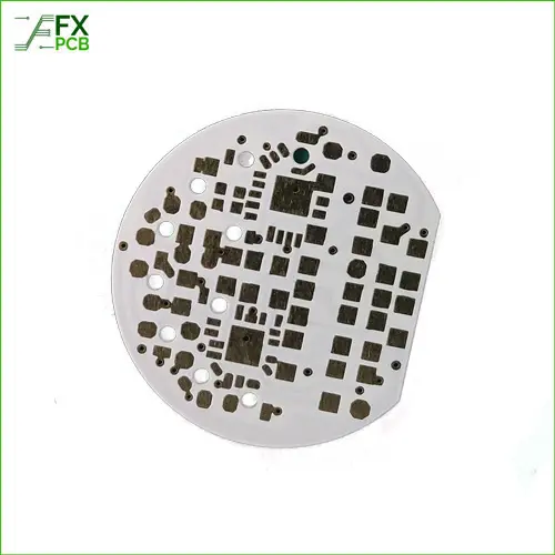
Before diving into design considerations, it’s essential to appreciate what a Ceramic PCB is and why it’s an ideal candidate for optimal thermal management. To define PCB, it is also called as Printed Circuit Board. They’re usually made of advanced materials that may include Aluminum Nitride and Aluminia. Compared to traditional PCB materials like FR4 or metal-core, ceramics offer a significantly higher thermal conductivity (24-170 W/mK, depending on the ceramic type).
Overheating and subsequent component failures can be avoided because to the board’s high thermal conductivity, which allows heat to be quickly distributed throughout the board and dissipated into the environment. Thus, the choice of Ceramic PCBs can directly impact the performance and longevity of electronic devices.
1. Material Selection
One of the most crucial aspects of designing Ceramic PCBs for optimal thermal management is the selection of appropriate ceramic materials. The two most common ceramic materials used are alumina and aluminium nitride, each with its unique benefits. Alumina, for instance, is more cost-effective and offers good electrical insulation. Aluminum nitride, is a great option for high-power electronics due to its strong heat conductivity. The choice between these materials primarily depends on the balance between cost and performance requirements of the project.
2. Mastering PCB Layer Stack-up
Delving into the architecture of a PCB, we find it consists of a strategic arrangement of insulating and conductive layers, aptly referred to as the layer stack-up. The beauty of designing Ceramic PCBs lies in the power of thermal management you hold within your hands once you master this layer stack-up design.
One tactical approach to designing an effective layer stack-up in a Ceramic PCB is the strategic placement of power and ground planes. Particularly, placing these close to the heat-generating components on the board is a clever tactic. Imagine these planes as diligent sentinels that guard against the enemy of excess heat. They fulfill this duty by acting as heat spreaders, diligently drawing away the heat from its source and dissipating it. This effective heat dispersion reduces the temperature at the source and significantly mitigates the formation of troublesome hotspots that could jeopardize the performance of your electronics.
3. The Art of Via Design
Dotted across the expanse of a PCB are tiny holes, known as vias. Unassuming as they may seem, these vias are vital bridges that enable electrical connection between the different layers of a PCB, contributing significantly to heat dissipation. In the world of Ceramic PCBs, you have the option of employing through vias. These special vias valiantly extend through the entire thickness of the board, forging connections where most needed.
In this context, the use of a conductive material to fill these vias is akin to adding a turbo boost to your thermal management strategy. Take copper, for instance. When used to fill vias, copper can establish an efficient thermal path, aiding in channeling heat away from high-power components and towards areas of lower thermal activity. It does not come without any complications. The design of these vias must take into account potential issues, such as the risks of thermal expansion mismatch and the need for pinpoint drilling accuracy.
4. Navigating Component Placement and Routing
Mapping out the placement of components and routing of traces on your Ceramic PCB is another crucial aspect that requires your keen attention. It’s comparable to setting up your team on a football field. You need to ensure that your high-power components, akin to your key players, are evenly distributed across the surface of your Ceramic PCB. This strategic distribution serves to prevent the buildup of heat in any single area, thus promoting an even temperature across the board.
When it comes to routing traces, the golden rule is to keep them thick and short, particularly for high current paths. Just like a well-lit highway enables smooth and swift movement of vehicles, these broad and short traces facilitate the efficient handling of high currents and augment heat dissipation.
5. Enhancing with Thermal Interface Materials (TIMs)
The final act in the drama of designing Ceramic PCBs for optimal thermal management is the entrance of Thermal Interface Materials, or TIMs. Picture TIMs as a layer of thermal adhesive that binds the PCB and the heat sink. By improving the thermal connection between these two, TIMs work silently in the background to maximize heat transfer, further tipping the balance in favor of efficient thermal management.
Not only do TIMs augment heat transfer, but they also serve as an additional safeguard against component failure. By effectively carrying heat away from the components and towards the heat sink, they significantly reduce the risk of your components overheating and failing. Thus, TIMs are the unsung heroes, the final piece of the puzzle in the grand scheme of optimal thermal management in Ceramic PCBs.