PCB Assembly Quote
Introduction to PCB Assembly
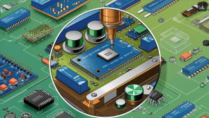
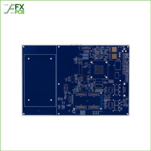
Microcircuits are one of the central elements of any electronic device for pcb assembly. They are fixed to the insulator plate by mounting printed circuit boards. Conductors are soldered to special tracks, which allow them to be included in a complex working network and establish communication with other contact nodes.
There are several mounting methods that are selected according to the type of device and its purpose:
(SMD) – installation in through holes.
(TNT) – surface mounting of printed circuit boards.
Mixed – this uses a combination of both through-hole mounting and surface mounting on the same board.
Surface mounting of printed circuit boards has a number of advantages, as it increases the functionality and at the same time, reduces the weight and size of the electronic product. Surface mounting is the fixing of components on the outer surface of the board.
The leads are soldered to the intended track, but do not go through it. This is the main difference from through-hole mounting. Thanks to surface mounting, electrically conductive circuits can be applied on both sides of the board without touching each other. This approach doubles the distance of the working surface for attaching contacts.
Through-hole Mounting
Through-hole mounting or through-hole mounting is the fastening of microcircuits through holes on the board. There is a solder of components in the metallized holes and their strong fastening. A distinctive feature of this method is the fastening of the elements – the conclusions of the components pass through the material of the insulator. Tubercles appear on the other side, they are then carefully cut off.
All types can be used as a separate assembly of printed circuit boards, and in a mixed form. If you need to create a complex microcircuit, then a mixed approach is often used – it allows you to achieve continuous operation of multilayer boards on one or more plates.
BENEFITS OF EACH BOARD MOUNTING METHOD
The company uses different methods of fixing elements on a dielectric plate – it is selected depending on the type of product. Each of the methods has its own characteristics, both disadvantages and advantages, so the choice in each case will always be individual.
Pros of Surface Mount PCBs
- It is easy to process plates – no need to drill, perform plating.
- Components and their outputs have less weight, more modest dimensions.
- The boards are used on each side and are smaller.
- Elements are fixed easily and reliably.
- The resulting product is compact.
- Chips can be batch processed in a professional oven.
Always Hire Professional PCB Assembly Company in China
Among the shortcomings of the surface method, there is a need for competent specialists and the availability of high-quality equipment, as well as the use of proven components. Our company employs qualified technologists, and has professional equipment for all stages of work, so we can easily avoid the shortcomings of SMD fixing components.
Benefits of TNT through-hole mounting
All contacts in the holes are subjected to reliable soldering.
The risk of overheating of the elements is reduced, they are less likely to be damaged and exfoliate.
It is possible to solder leads to the inner surface of the plate.
The disadvantages of such fixation are the large size and weight of individual components, the finished product weighs more, it is necessary to process the boards after installation, and the time for high-speed signals is reduced.
The through-hole fastening method is more relevant for manual processing. As a rule, it is used for particularly complex boards or a small-scale production batch.
PCB ASSEMBLY PROCESSES
The technology of mounting printed circuit boards is divided into two general stages:
Installation of elements on the substrate – capacitors, light indicators, compartments for batteries, power buttons, levers, etc.
Soldering components to a printed circuit board
Each of the PCB assembly processes has its own characteristics and difficulties. Several stages allow you to achieve a complete installation of elements and include different types of materials and components in the process. It also adapts the installation to the desired production volumes and provides a high level of reliability, protecting against rejects.
PCB ASSEMBLY – ADVANCED STEPS:
- The insulating substrate and the surface of the material are prepared for processing.
- Flux and molten metal are applied for solder.
- Solder melts to form soldered items.
- Finished compounds are washed.
- Product testing and verification.
Final Thought
Features of the pcb assembly line can affect the number of stages, sometimes they can be combined, or some of them are completely excluded.
It is important that the equipment manager and process engineer understand how important it is to follow all the steps and rules of installation to create a reliable and durable product. Also, the steps may vary depending on the type of installation chosen – surface or through holes.