Printed circuit boards (PCBs) are an integral part of modern electronic devices, providing the foundation for interconnecting components and enabling the flow of electrical signals. Copper plays a vital role within a PCB as the primary material for creating conductive pathways, also known as traces. The thickness of the copper layers on a PCB, called PCB copper thickness, holds significant importance in the design and performance of the circuit board.
This comprehensive guide delves into the world of PCB copper thickness and its crucial role in PCB design. We will explore PCB copper thickness and its implications on electrical performance, current carrying capacity, heat dissipation, and signal integrity. Furthermore, we will uncover the importance of understanding and selecting the appropriate copper thickness to ensure the reliability and functionality of PCBs in various applications.
Additionally, this guide will expand beyond PCB copper thickness to shed light on the broader concept of 4-layer PCB stackup and PCB panel design. Understanding the PCB stackup is essential for achieving desired electrical, mechanical, and thermal characteristics, while panel design involves optimizing the arrangement and manufacturing of multiple PCBs on a single PCB panel. We will explore the significance of PCB stackup and panel design in ensuring efficient production, cost-effectiveness, and reliable operation of electronic devices.

FX PCB can provide the ALN(Aluminum oxide) and AIO203(Aluminum Nitride) Ceramic PCB, we can make ENEPIG, ENIG, Immerison silver surface,you can check the material datesheet and our capability from the below tables.
The ceramic circuit board has the following characteristics: high-temperature resistance, high electrical insulation, low dielectric constant, low dielectric loss, high thermal conductivity, good chemical stability, and the thermal expansion is almost can be coefficients of components.
Ceramic PCB is actually made of electronic ceramic materials and can be made into various shapes.
Copper thickness specifications refer to the specific measurement of copper layer thickness on a PCB. It is typically expressed in ounces per square foot (oz/ft²) or micrometers (μm). Understanding these specifications is crucial for PCB designers as it allows them to determine the appropriate copper thickness for their specific application.
When specifying copper thickness, it is important to consider both the outer and inner layers of copper thickness. The outer layer copper thickness is often more critical as it directly affects the trace width and spacing. In contrast, the inner layer copper thickness influences the PCB’s overall electrical and thermal performance.
Copper thickness specifications may vary based on different PCB manufacturers’ manufacturing capabilities and standards. It is essential to communicate clearly with the manufacturer and verify their capabilities to ensure the desired copper thickness can be achieved during fabrication. By understanding the copper thickness specifications, designers can effectively communicate their requirements and provide the desired performance and functionality of the PCB.
Several factors influence the selection of copper thickness for a PCB design. It is crucial to consider these factors to determine the optimal copper thickness that meets the application’s specific requirements. Some key factors include:
The amount of present the PCB traces need to carry is a crucial consideration. Higher current levels necessitate thicker copper layers to minimize resistive losses and prevent overheating.
The circuit’s complexity and the traces’ density play a role in selecting copper thickness. Designs with intricate and dense trace patterns may require thinner copper layers to accommodate fine trace widths and spacing.
If the PCB is expected to dissipate a significant amount of heat, thicker copper layers are beneficial. Thicker copper helps spread heat across the board more efficiently, preventing localized hotspots and ensuring optimal thermal management.
Copper thickness can impact the overall cost of PCB fabrication. Thicker copper layers incur higher manufacturing costs due to increased material usage and processing requirements. Therefore, cost constraints may influence the selection of copper thickness.
The manufacturing capabilities and processes available at the chosen PCB manufacturer may limit the achievable copper thickness. Working closely with the manufacturer is crucial to ensure the copper thickness selected is within their capabilities.
With applications and advantages, standard copper thickness options are available for PCB designs. Some of the typical copper thickness options include 1 oz/ft² (35 μm), 2 oz/ft² (70 μm), and 3 oz/ft² (105 μm).
It’s important to note that these are just some standard copper thickness options, and specific applications may require customized thicknesses based on the unique requirements of the design. By understanding the legal copper thickness options and their respective applications, designers can make informed decisions to achieve optimal performance and reliability in their PCB designs.
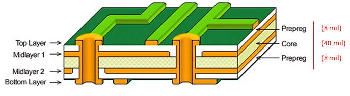
4-layer PCB stackup refers to a printed circuit board configuration comprising four conductive materials separated by insulating layers. This stackup offers more flexibility and functionality than single or double-layer PCBs, making it suitable for various applications ranging from consumer electronics to industrial controls.
In PCB panel design, multiple 4-layer PCBs are arranged and manufactured on a single panel. Penalization offers several advantages, including improved production efficiency, reduced manufacturing costs, and easier handling and assembly of PCBs during the manufacturing process. Proper stackup design is essential to ensure the success of penalization.
The top layer is the primary signal layer and contains most of the circuitry, including components, traces, and solder mask openings. This layer provides the necessary interconnectivity and functionality for the PCB.
In a 4-layer stackup, two inner signal layers are typically sandwiched between the internal power and ground planes. These signal layers allow for additional routing space, enabling complex and dense circuit designs while maintaining signal integrity and minimizing noise.
The inner and ground planes are essential for power distribution, decoupling, and noise reduction. These planes provide a stable reference potential and low impedance for power and ground connections throughout the PCB. They enhance the overall signal integrity, reduce electromagnetic interference (EMI), and offer improved thermal management.
The bottom layer of the PCB stackup is another signal layer, similar to the top layer. It provides additional routing space for components, traces, and solder mask openings, completing the circuitry of the PCB.
Adhere to the specific panelization guidelines provided by the PCB manufacturer. These guidelines may include panel size, spacing, and routing constraints to ensure proper assembly and efficient manufacturing.
Maintain good sign and power integrity by carefully planning the placement of critical components, signal traces, and power distribution. Ensure controlled impedance for high-speed signals and adequate power plane capacity for stable power delivery.
Consider thermal management aspects, especially if the PCBs in the panel will experience high-power components or heat-generating areas. Adequate spacing between PCBs, thermal vias, and heat dissipation techniques can help dissipate heat effectively.
Optimize the stackup design for manufacturability and yield. Consider the capabilities and limitations of the PCB manufacturing process, such as layer alignment, material availability, and PCB panel handling during assembly.
By carefully designing the 4-layer PCB stackup for panelization and considering factors such as signal integrity, power distribution, thermal management, and manufacturability, you can achieve efficient production, cost-effectiveness, and reliable operation of the PCBs in a panelized configuration. Collaboration with experienced PCB manufacturers can provide valuable insights and guidance throughout the panel design process.
PCB stackup refers to arranging and configuring multiple layers within a printed circuit board. A PCB typically consists of several layers, each serving a specific purpose and contributing to the overall functionality of the board. The stackup defines these layers’ order, sequence, and characteristics, including signal layers, power planes, and ground planes.
The PCB stackup is crucial as it determines the board’s electrical, mechanical, and thermal properties. It influences impedance control, signal integrity, electromagnetic compatibility (EMC), power distribution, and heat dissipation. By carefully designing the stackup, designers can optimize the performance and reliability of the PCB for its intended application.
Various layers are strategically arranged in a typical PCB stackup to fulfill specific functions. Here are the commonly used layers and their functionalities:
Signal layers contain the conductive traces that carry electrical signals between different components on the PCB. These layers interconnect the various electronic components and ensure proper signal propagation. Signal layers may include top and bottom layers and inner layers for complex multilayer designs.
Power and ground planes are dedicated layers that provide a stable power distribution and a low-impedance return path. Power planes deliver power to components, while ground planes serve as a reference potential and help minimize noise and interference. These planes enhance signal integrity, reduce electromagnetic interference (EMI), and facilitate effective decoupling and bypassing of components.
Additional inner signal layers between the power and ground planes for multilayer PCBs can be included. These layers provide additional routing space for signals, allowing for increased density and complexity in the design.
Prepreg layers consist of insulating material impregnated with resin and bond the core layers together. Core layers are made of solid insulating material, such as FR-4, and provide structural strength and rigidity to the PCB
Choosing the appropriate PCB stackup is crucial for meeting the design requirements and achieving optimal performance. The selection process involves considering factors such as signal integrity, power delivery, thermal management, and manufacturability. Here are some key considerations when choosing the right stackup for your design:
Determine your design’s required impedance control and signal integrity characteristics. Consider the type of signals, signal speeds, and potential noise sources. A stackup with controlled impedance and proper signal routing techniques should be chosen.
Assess the thermal characteristics of your design, especially if it involves high-power or heat-sensitive components. A stackup with proper thermal vias, heat dissipation layers, and efficient thermal paths can help manage and dissipate heat effectively.
By carefully analyzing these factors and understanding your design requirements, you can make informed decisions in choosing the most suitable PCB stackup and collaborating with experienced.

I am Peter Gong. I have been working in PCB and PCBA industry for 15+ years now. I have been a part of the PCB revolution with my dedication to circuit board technologies and creative ideas. I write in FX PCB to impart my knowledge on PCB and PCBA for all circuit board lovers, manufacturers, and users.
WhatsApp us