What Is a Glass PCB?
A glass PCB is a printed circuit board built on a solid sheet of glass instead of a conventional organic laminate. Copper circuitry is formed directly on the glass surface, and plated through-glass vias (TGV) connect the layers. Because the substrate itself is glass, the finished board can be transparent, extremely flat, and dimensionally stable.
It helps to be clear about what a glass PCB is not. FR4 — the standard PCB material — is woven fiberglass cloth impregnated with epoxy resin. Despite the word “glass” in “fiberglass,” an FR4 board is an opaque resin composite; a glass PCB uses a solid glass panel as the core material, which gives it a completely different set of properties: optical transparency, a much smoother surface for fine-line circuitry, low dielectric loss for high-frequency signals, and a coefficient of thermal expansion close to that of silicon.
Ceramic PCBs sit at the other end of the range. Ceramics (such as alumina and aluminum nitride) are opaque and are chosen mainly for heat conduction and high-temperature service. Glass PCBs are chosen when transparency, flatness, fine lines, and signal quality matter more than raw thermal conductivity — for example in lighting, displays, sensors, and design-led electronic products.
FX PCB manufactures custom glass PCBs in Shenzhen, China, in 1–6 layers and thicknesses from 0.3mm to 3.0mm, with line width and spacing down to 0.05mm. Send us your Gerber files and we will return a quote in 1–2 working days.
Glass PCB Capabilities
| Parameter | Specification |
|---|---|
| Layers | 1–6 |
| Min. line width / spacing | 0.05 / 0.05 mm |
| Board thickness | 0.3–3.0 mm |
| Copper foil | 1–3 oz |
| Warpage | ≤0.5% (at 1.6mm thickness, 300 × 300mm) |
| Thermal conductivity | 0.4–2 W/m·K |
| Routing tolerance | ±0.05 mm (laser) |
| Barrel copper thickness | 10–30 μm |
| Hole position tolerance | ±0.05 mm |
| Min. via | 50 μm |
| Min. mechanical drill | 0.5 mm |
| Surface finishes | OSP, ENIG (immersion nickel gold), ENEPIG (immersion nickel palladium gold), immersion tin |
| Finish thickness | Gold plating: Ni 4–6 μm, Au 0.1–0.5 μm; immersion gold: Ni 5–6 μm, Au 0.02–0.12 μm; immersion tin: 3–5 μm |
| Min. solder mask opening | 0.15 mm |
Types of Glass PCBs We Make
Transparent Glass PCBs
Our most requested glass product. Circuitry is built on clear glass so the board stays see-through where there are no traces — used in LED lighting, display backlights and covers, touch and sensor panels, and products where the board itself is part of the design. See our transparent glass PCB products:
Single-Sided and Double-Sided Glass PCBs
One or two copper layers on a glass core for simpler lighting, signage, and sensor circuits — the most economical way to use glass where transparency or a flat, rigid surface is the main requirement.
Multilayer Glass PCBs (Up to 6 Layers)
For denser designs, we build glass PCBs up to 6 layers with plated through-glass vias down to 50 μm, laser routing held to ±0.05 mm, and warpage controlled to ≤0.5%.
Glass Core Substrates for Advanced Packaging
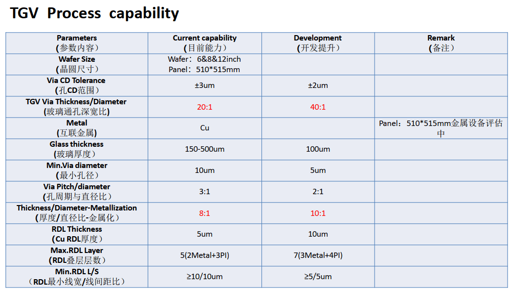
We also produce glass core substrates for advanced packaging. Our process flow is built for this work: TGV drilling with vias down to 50 μm, via metallization, LDI patterning at 0.05mm line width and spacing, and an RDL (redistribution layer) routing step in the back-end process. The glass core is flat and dimensionally stable, with thermal expansion close to silicon. Send us your design and we will review it against our process window.
Glass Types We Work With
Glass types we work with include tempered glass, float glass, quartz glass, and sapphire glass — tell us what your design needs and we will match the glass type to the application.
How Glass PCBs Are Made
Glass boards follow their own process flow — drilling, imaging, and singulation are all different from FR4. Our production runs 16 steps:
Front-End Process
- Glass Cutting — the raw glass panel is cut to the working panel size.
- TGV Drilling — through-glass via holes are formed in the panel.
- Via Metallization — the via walls are made conductive so layers can connect.
- Thick-Film Copper — a copper layer is built up on the glass surface.
- Blind Via — blind vias for the first interconnect level are formed.
- LDI Patterning — the circuit image is written directly by laser direct imaging, which is how 0.05mm lines are held.
- Organic Bonding — layers are bonded together for multilayer builds.
- Blind Via II — the second blind-via step completes the layer interconnects.
Back-End Process
- RDL Routing — redistribution-layer wiring is formed for fine-pitch fan-out.
- In-Line Test — circuitry is checked electrically during the process, not only at the end.
- Solder Mask — solder mask is applied and imaged (minimum mask opening 0.15mm).
- Surface Finish — the pads receive the specified finish: OSP, ENIG, ENEPIG, or immersion tin.
- Laser Dicing — individual boards are singulated from the panel by laser, which keeps edges clean and holds the ±0.05mm routing tolerance.
- Precision Test — final dimensional and electrical verification.
- AVI Inspection — automated visual inspection checks every board’s appearance and pattern.
- Packaging — finished boards are packed for shipment.

Applications
- Lighting — transparent and decorative LED boards, light-guide and architectural lighting, illuminated signage, where the board should not block or discolor the light.
- Displays — display backlight boards, transparent display elements, and Mini/Micro LED carriers that benefit from a flat, clear substrate.
- Sensors — optical and environmental sensor boards where the substrate must pass light or stay chemically inert and sealed.
- Design-Driven Electronics — consumer and architectural products where the circuit board is visible and transparency is part of the product design.
What Affects Glass PCB Cost
We quote every glass PCB individually, but the price is driven by a predictable set of factors:
- Glass type — the glass material itself is a major cost component, and different glass types differ in price.
- Board size and panel utilization — larger boards and poor panel fit raise the cost per piece.
- Thickness — our range is 0.3–3.0mm; very thin and very thick glass both need more careful handling.
- Layer count — a single-sided board and a 6-layer build go through very different process routes (see the 16 steps above).
- Line width and via size — 0.05mm lines and 50 μm vias are at the fine end of the process window and cost more than relaxed designs.
- Surface finish — OSP is the economical option; gold finishes (ENIG, ENEPIG, gold plating) add material cost.
- Quantity — prototypes carry the setup cost over few pieces; unit price falls as volume rises.
If you send us your Gerber files and quantity, we will quote the actual design rather than a guess — quotes are returned in 1–2 working days.
FAQ
What is the difference between a glass PCB and an FR4 PCB?
FR4 is woven fiberglass cloth set in epoxy resin — an opaque organic laminate. A glass PCB is built on a solid glass sheet, so it can be transparent, flatter, and smoother for fine-line work, and it behaves differently at high frequencies. FR4 remains cheaper and tougher for general-purpose boards; glass is chosen when transparency, flatness, or signal quality is the point.
What thicknesses and layer counts can you produce?
Board thickness from 0.3mm to 3.0mm, and from 1 to 6 layers.
How fine can the circuitry and vias be?
Minimum line width and spacing are 0.05/0.05mm. The smallest via is 50 μm, and the smallest mechanical drill is 0.5mm.
Which surface finishes are available?
OSP, ENIG, ENEPIG, and immersion tin. Finish thicknesses: gold plating Ni 4–6 μm with Au 0.1–0.5 μm; immersion gold Ni 5–6 μm with Au 0.02–0.12 μm; immersion tin 3–5 μm.
How do I get a quote for a glass PCB?
Send us your Gerber files, the layer count and thickness, the surface finish, and the quantity you need. We review every glass design against our process window and return a quote in 1–2 working days.
Get a Quote
Send us your Gerber files for a quote in 1–2 working days — from single prototypes to production runs.
Industry Background: Why Glass Substrates Are Getting Attention
The sections above cover what we make and how we make it. The article below, first published as an industry overview, explains why the wider electronics industry is moving to glass.
Introduction: Hitting a Wall with Traditional Materials?
If you’re working in AI, high-performance computing, or 5G, you’ve likely felt the bottleneck. For years, the industry has relied on organic substrates like FR-4 and ABF. But as we push for more speed, power, and miniaturization, these traditional materials are starting to fail us. The problems are clear: signal loss at high frequencies, chips warping from heat, and a physical limit on how much we can connect in a single package.
So, what’s the solution? Look no further than Glass PCBs.
This isn’t just a minor upgrade. It’s a fundamental shift. As a specialized glass PCB manufacturer, we see this technology as the key to unlocking the next generation of electronics. Let’s dive into why the biggest names in tech are betting on glass.
Why the Industry is Switching to Glass PCBs
Why are companies like Intel and NVIDIA re-engineering their future products around glass? The advantages are simply too significant to ignore.
-
Crystal-Clear Signal Integrity: Imagine a highway with no friction. That’s what signals experience on a Glass PCB. With a lower dielectric constant and dissipation factor than organic materials, glass drastically reduces power loss and crosstalk. This is a game-changer for high-speed RF and millimeter-wave applications in 5G and beyond.
-
Rock-Solid Stability: Silicon and organic materials expand at different rates when heated, causing stress and warping. Glass has a nearly identical thermal expansion coefficient to silicon. This means Glass PCBs stay flat and stable, enabling larger, more powerful chips and dramatically improving long-term reliability.
-
Unprecedented Interconnect Density: The surface of glass is incredibly smooth, allowing for ultra-fine circuit lines. Combined with Through-Glass Vias (TGV)—which are smaller and can be placed closer together than traditional holes—a glass PCB manufacturer can pack an immense number of connections into a tiny area. This density is critical for advanced multi-chip packages and HPC.
-
Built-in Thermal and Mechanical Benefits: Glass dissipates heat more effectively than many standard substrates, helping to keep powerful chips cooler. Its inherent rigidity also provides a stable foundation for manufacturing, especially on large, panel-level formats.
-
See-Through and Sealed: For applications like Mini/Micro LED displays or advanced sensors, the optical transparency and natural impermeability of glass offer unique benefits that organic materials can’t match.
The Giants Are All-In: Industry Momentum for Glass Substrates
You don’t have to take our word for it. The biggest players in tech are publicly committing to this future:
-
Intel: After a decade of R&D, they plan to launch glass-based processors by 2026-2030, stating it allows them to pack more transistors into a single package.
-
NVIDIA & AMD: Both are actively testing and plan to integrate glass substrates to manage the power and bandwidth demands of next-gen AI chips.
-
Samsung: Is building a prototype line with a target for mass production by 2026.
-
The Ecosystem: From Apple and Corning to BOE, the investment in glass core technology is massive and global.
For the step-by-step process we run in production, see “How Glass PCBs Are Made” above.

The Road Ahead: Challenges and Opportunities
Of course, pioneering a new technology comes with hurdles. Glass is brittle, requiring careful handling. Building complex, multi-layer boards is still more challenging than with organics. And the supply chain is still maturing.
But as a forward-thinking glass PCB manufacturer, we are actively solving these challenges. The immense performance gains make the pursuit unquestionably worthwhile. The question isn’t if glass will become mainstream, but when.
Conclusion: Your Next Project Deserves a Glass Foundation
The limitations of traditional materials are clear. The future of high-performance electronics is being built on glass. By partnering with a skilled glass PCB manufacturer now, you can ensure your products are at the forefront of this revolution.
Ready to explore how a Glass PCB can power your innovation? Contact us today for a expert consultation and see the difference a clear advantage can make.