Introduction: Hitting a Wall with Traditional Materials?
If you’re working in AI, high-performance computing, or 5G, you’ve likely felt the bottleneck. For years, the industry has relied on organic substrates like FR-4 and ABF. But as we push for more speed, power, and miniaturization, these traditional materials are starting to fail us. The problems are clear: signal loss at high frequencies, chips warping from heat, and a physical limit on how much we can connect in a single package.
So, what’s the solution? Look no further than Glass PCBs.
This isn’t just a minor upgrade. It’s a fundamental shift. As a specialized glass PCB manufacturer, we see this technology as the key to unlocking the next generation of electronics. Let’s dive into why the biggest names in tech are betting on glass.
Why the Industry is Switching to Glass PCBs
Why are companies like Intel and NVIDIA re-engineering their future products around glass? The advantages are simply too significant to ignore.
Crystal-Clear Signal Integrity: Imagine a highway with no friction. That’s what signals experience on a Glass PCB. With a lower dielectric constant and dissipation factor than organic materials, glass drastically reduces power loss and crosstalk. This is a game-changer for high-speed RF and millimeter-wave applications in 5G and beyond.
Rock-Solid Stability: Silicon and organic materials expand at different rates when heated, causing stress and warping. Glass has a nearly identical thermal expansion coefficient to silicon. This means Glass PCBs stay flat and stable, enabling larger, more powerful chips and dramatically improving long-term reliability.
Unprecedented Interconnect Density: The surface of glass is incredibly smooth, allowing for ultra-fine circuit lines. Combined with Through-Glass Vias (TGV)—which are smaller and can be placed closer together than traditional holes—a glass PCB manufacturer can pack an immense number of connections into a tiny area. This density is critical for advanced multi-chip packages and HPC.
Built-in Thermal and Mechanical Benefits: Glass dissipates heat more effectively than many standard substrates, helping to keep powerful chips cooler. Its inherent rigidity also provides a stable foundation for manufacturing, especially on large, panel-level formats.
See-Through and Sealed: For applications like Mini/Micro LED displays or advanced sensors, the optical transparency and natural impermeability of glass offer unique benefits that organic materials can’t match.
The Giants Are All-In: Industry Momentum for Glass Substrates
You don’t have to take our word for it. The biggest players in tech are publicly committing to this future:
Intel: After a decade of R&D, they plan to launch glass-based processors by 2026-2030, stating it allows them to pack more transistors into a single package.
NVIDIA & AMD: Both are actively testing and plan to integrate glass substrates to manage the power and bandwidth demands of next-gen AI chips.
Samsung: Is building a prototype line with a target for mass production by 2026.
The Ecosystem: From Apple and Corning to BOE, the investment in glass core technology is massive and global.
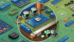
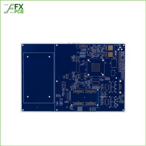
How a Glass PCB is Made: A Peek into the TGV Process
As an experienced glass PCB manufacturer, our expertise lies in mastering the complex process of creating Through-Glass Vias (TGV). Here’s a simplified look:
Laser-Induced Etching (The “Drilling”): We use ultra-fast lasers to subtly alter the glass’s structure in precise locations. A follow-up chemical bath then etches away the modified areas, creating incredibly clean and smooth micro-vias. This is the gold standard for TGV formation.
Metallization (Making it Conductive): This is a critical step. We use a process called PVD Sputtering to coat the entire panel, including the deep, narrow via walls, with a thin, uniform layer of metal (like Titanium and Copper). This creates the foundational seed layer for conductivity.
Electroplating (Building the Pathways): We then build upon that seed layer, using electroplating to fill the vias with solid copper and form the surface circuitry. This creates robust, low-resistance electrical pathways.
Fine-Line Patterning (The Final Touch): Using advanced photolithography, we print and etch the final, intricate circuit pattern onto the surface, completing the Glass PCB.


The Road Ahead: Challenges and Opportunities
Of course, pioneering a new technology comes with hurdles. Glass is brittle, requiring careful handling. Building complex, multi-layer boards is still more challenging than with organics. And the supply chain is still maturing.
But as a forward-thinking glass PCB manufacturer, we are actively solving these challenges. The immense performance gains make the pursuit unquestionably worthwhile. The question isn’t if glass will become mainstream, but when.
Conclusion: Your Next Project Deserves a Glass Foundation
The limitations of traditional materials are clear. The future of high-performance electronics is being built on glass. By partnering with a skilled glass PCB manufacturer now, you can ensure your products are at the forefront of this revolution.
Ready to explore how a Glass PCB can power your innovation? Contact us today for a expert consultation and see the difference a clear advantage can make.