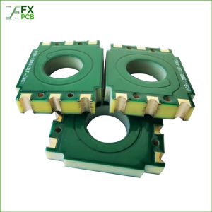
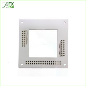
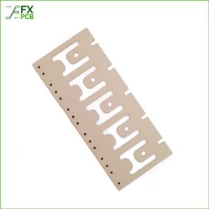
Description
What is a thick film Ceramic PCB?
Thick film is the thickness of the conductor layer of the Ceramic PCB. Generally speaking, the thickness should be over 10um(micrometers) at least, ranging between 10- 13um. It is thicker than the sputtering technology used in thin film ceramic PCB, but the thickness is still thinner than DBC ceramic PCB or FR4 boards. Using the thick film technology, Ceramic PCBs are manufactured through printing and a high-temperature sintering process, which can allow the resistor, capacitor, conductor, semiconductor, and switchable conductors to be integrated onto the Ceramic substrate. Meanwhile, with the thick film technology, we can make all of the resistors the same value on the board, or set different values for the different resistors on the same PCB.

How to make a thick film Ceramic PCB?
the metal paste is screen-printed onto the ceramic substrate to form the conductive wiring layer. Then, the printed ceramic substrate undergoes binding and sintering, bonding the metal layer tightly to the ceramic base and forming the final thick film Ceramic substrate
Bond Strength between Metal Wiring Layer and Ceramic Substrate
The adhesion of the metal wiring layer to the ceramic substrate is a characteristic of thick film ceramic substrates. The metal layer is closely bonded to the ceramic substrate to avoid peeling. Thick-film Ceramic PCB thus formed have good resistance to heat shock, good thermal stability, and can also be used in high-temperature situations.
Metal Wiring Layer Thickness
The metal wiring layer on the thick-film ceramic substrate has a thickness of about 10–20 μm (Commonly, if a thicker metal layer is required, multiple screen-printing steps are performed). The thickness of the metal layer is substantially uniform, meeting the standards for most electronic packaging needs.
What is the difference between Thin-film and Thick-film Ceramic Substrates?
The ceramic substrates provide mechanical support and electrical insulation for components in electronic packaging. They can be classified as thin-film and thick-film ceramic substrates based on the manufacturing processes and thickness, and each of them has its own properties and applications. Let’s find out the difference roughly:
01 Difference in Thickness
- Thin-film ceramic PCB is normally below 10um thickness (even under 1um), which makes them ideal for high-density integration and microelectronics.
- Thick-film Ceramic PCB should be above 10 um, and it is better suited for power electronics and larger components.
02 Difference in Manufacturing Processes
- Thin-film Ceramic PCB can allow the precise thickness control and fine patterning, as they use vacuum evaporation, sputtering, etc
- Thick-film Ceramic PCB are good for complex patterns with less precise thickness control, as it made by screen printing
03 Difference in Applications
- As thin-film Ceramic PCB are thin, uniform, and precise, It used mostly in high-frequency, high-speed, and high-power electronics
- Thick-film Ceramic PCB have strong thermal management and mechanical strength, so they are preferred for power electronics, automotive electronics, and other applications
Summary:
No matter which you choose, the thick film Ceramic or the thin film Ceramic, we need to understand the difference in thickness, manufacturing processes, and applications first, so you can make the right choice. Contact FX PCB for more questions regarding your Ceramic PCB