RF (Radio Frequency) PCBs are the backbone of modern wireless communication systems, radar equipment, satellite technology, and countless other applications that rely on the efficient transmission and reception of high-frequency signals. To achieve the desired performance in these systems, it’s essential to understand the intricacies of RF PCB design and follow specific guidelines. In this comprehensive article, we will delve into the world of RF PCBs, exploring their significance, design principles, and why rf pcb metters.

The modern-day electronics world depends heavily on the Printed Circuit Boards (PCBs) as its backbone. A PCB is a medium to transfer the current through its copper pathway and it dissipates the heat to keep the tiny yet highlycomplex electronic equipment on it in perfect condition.
If you are to get the best PCBA and PCB for your digital devices, you have to know this PCB assembly process thoroughly. FX PCB with its years of experience understands this need and thus, we present you the detailed guideline.
FX PCB dont follow the standerd manufacturing process is no exception to it. Our process includes solder pasting on the PCB base, placing the electronic components in the right place, soldering them with the PCB, checking the accuracy, final inspection, and delivery to customers.
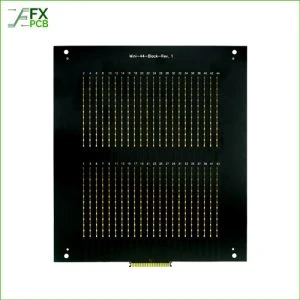
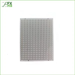
RF PCB stands for Radio Frequency Printed Circuit Board. It is a type of printed circuit board (PCB) that is specifically designed and optimized for applications involving radio frequency signals. RF PCBs are used in various electronic devices and systems that transmit, receive, or process RF signals, such as wireless communication devices, radar systems, satellite communication equipment, and more.
High-Frequency Operation: RF PCBs are designed to operate at high frequencies, typically in the radio frequency range, which can extend from a few megahertz (MHz) to several gigahertz (GHz).
Low Signal Loss: Minimizing signal loss is crucial in RF applications. RF PCBs are designed with low-loss dielectric materials and controlled impedance traces to maintain signal integrity.
Impedance Matching: Impedance matching is essential to ensure maximum power transfer between RF components. RF PCBs are carefully designed to maintain the desired impedance levels for the entire RF circuit.
Isolation and Grounding: Proper isolation and grounding techniques are employed to reduce interference and noise in RF circuits. This helps maintain the integrity of the RF signals.
PCB Material Selection: The choice of PCB material is critical in RF PCB design. Materials like Rogers or PTFE-based substrates are often used due to their low dielectric constant and low loss properties at high frequencies.
Trace Geometry: The width, spacing, and geometry of traces on an RF PCB are optimized to minimize signal reflections and losses. Transmission line structures like microstrips or striplines are commonly used.
Component Placement: Careful placement of RF components on the PCB is essential to reduce parasitic capacitance and inductance, which can affect circuit performance.
RF Testing: RF PCBs often undergo rigorous testing and validation to ensure that they meet the desired performance specifications, including testing for impedance matching, signal quality, and power handling capability.
RF PCB design is a specialized field that focuses on designing circuit boards for applications involving high-frequency radio frequency signals. To ensure the optimal performance of RF PCBs, designers follow specific guidelines and principles:

RF (Radio Frequency) PCBs are integral to the functioning of modern wireless communication and high-frequency electronic devices. Their significance lies in their ability to handle radio frequency signals with precision and efficiency.
These specialized PCBs are engineered to minimize signal loss, maintain impedance matching, and reduce electromagnetic interference, ensuring reliable data transmission in applications such as smartphones, Wi-Fi routers, radar systems, and satellite communication. RF PCBs also enable the integration of antennas and high-frequency components, allowing for compact and space-efficient designs, ultimately contributing to the advancement of wireless technology.
Furthermore, the stringent quality control and testing processes associated with RF PCB manufacturing guarantee that these boards meet the demanding requirements of high-frequency applications. Whether in consumer electronics or critical communication systems, RF PCBs play a pivotal role in supporting the seamless transmission of data and signals, making them an indispensable component in the world of wireless technology.

I am Peter Gong. I have been working in PCB and PCBA industry for 15+ years now. I have been a part of the PCB revolution with my dedication to circuit board technologies and creative ideas. I write in FX PCB to impart my knowledge on PCB and PCBA for all circuit board lovers, manufacturers, and users.
WhatsApp us