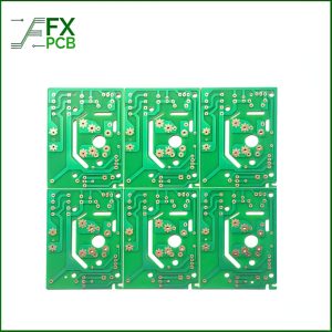
One domain witnessing significant progress in the technological world is Printed Circuit Board (PCB) manufacturing. This field has experienced several remarkable transformations over the past few years, with more changes forecasted on the horizon. This article will explore the emerging technologies and trends currently shaping the PCB manufacturing industry.
A PCB is like the nervous system of any electronic device. It interconnects and mechanically supports electronic components using conductive pathways, signal traces, or tracks etched from copper sheets laminated onto a non-conductive substrate. The complexity and performance requirements of contemporary electronics have pushed PCB manufacturers to seek new solutions, methodologies, and technologies.
Table of Contents
Our Recommended Rogers PCB
Rogers PCB is mostly used in high-frequency and high-power applications such as RF and microwave. the Rogers material normally has the advantages of low dielectric loss, stable dielectric constant, high thermal conductivity, thermal stability, etc. That’s why there are so many engineers and manufacturers choosing Rogers as the PCB material..
Technologies and Trends in PCB Manufacturing
Delving into Miniaturization
Today, compactness isn’t just a consumer preference – it’s a necessity driven by advancements across sectors like aerospace, medical technology, and automotive. The age of wearable technology, micro-implants, and nano-drones is upon us, and powering these innovations requires an unprecedented level of intricacy and precision in PCB design.
As electronic devices shrink, the demand for smaller, yet equally effective, circuit boards is skyrocketing. PCB manufacturers are rising to this challenge with impressive agility and innovation, focusing primarily on High-Density Interconnect (HDI) technology. HDI technology has been nothing short of a game-changer in the industry, enabling the creation of PCBs with finer lines and spaces, smaller vias, and capture pads. This technology has quite literally opened up new dimensions in PCB design, allowing manufacturers to fit more components into limited areas. As a result, we’re now seeing PCBs that not only meet the size requirements but also enhance device performance through faster signal transmission, reduced signal loss, and lower susceptibility to environmental damage.
The Flexibility Paradigm in Electronics
Bend it like never before – this could well be the motto in the electronics industry today as the advent of flexible electronics heralds a revolution in PCB manufacturing. This remarkable technology, characterized by thin, light, and bendable PCBs, is stretching the boundaries of what’s possible in electronics design. As the name suggests, flexible PCBs bring an exceptional degree of flexibility to device design, enabling the integration of electronics into unconventional shapes and forms.
Imagine wearable tech that seamlessly blends with the contours of your body, or tiny drones equipped with flexible electronics capable of withstanding challenging flight maneuvers. These are no longer science fiction but are becoming a reality, thanks to flexible PCBs. Recognizing the potential of this technology and its likely mainstream adoption in the near future, PCB manufacturers are proactively scaling up their capabilities. They’re investing in specialized equipment and developing the required expertise to cater to the growing demand for flexible PCBs, preparing to ride the wave of this exciting trend.
AI and Machine Learning in PCB Manufacturing
Think of PCB manufacturing as a symphony. Every stage, every process, needs to perform harmoniously to produce a masterpiece – a PCB that delivers on performance and reliability.
These technologies are all set to create a significant shift in PCB manufacturing, changing the way each stage of the process is managed. AI and machine learning are being leveraged to automate the inspection processes, which are integral to ensuring the quality and reliability of PCBs. They’re helping identify defects that could otherwise escape the human eye, enabling manufacturers to rectify issues before they escalate into major problems.
Moreover, AI’s predictive capabilities have opened up new possibilities in maintenance and quality assurance. Predictive analytics, powered by AI, is helping PCB manufacturers foresee potential issues in the manufacturing process.
Environmental Sustainability in PCB Manufacturing
Environmental sustainability is a driving force that is rapidly influencing the course of the PCB manufacturing industry. Global awareness and appreciation for sustainable practices have risen dramatically over the past decade, with both consumers and regulatory bodies urging industries to minimize their environmental footprints. This momentum hasn’t left the PCB manufacturing sector untouched.
PCB manufacturers are finding themselves at a critical junction where environmental considerations are not just good-to-have but essential to their operational and business strategies. Consequently, an industry-wide paradigm shift towards green manufacturing practices is underway.
Such a transition of using bio-resins and bio-plastic in PCB manufacturing doesn’t only align with the sustainability narrative but can also provide unique benefits such as improved insulation properties.

Rising Demand for High-Frequency PCBs
5G technology has driven high-frequency PCB demand. Modern wireless communication systems need to transmit massive amounts of data quickly and reliably, making high-frequency PCBs indispensable.
PCB makers are investing in R&D to discover new materials and enhance manufacturing methods to meet increased demand. High-frequency PCBs require specialized materials (Ceramics, PTFE, etc) that can handle rapid signal transmission with minimal loss.
In addition to materials, the manufacturing processes also need an upgrade. Precision is key when producing high-frequency PCBs as even minor defects can result in significant performance issues.
Embedded Components Technology (ECT) in PCB Design
The continual pursuit of smaller, lighter, yet more powerful electronic devices has led to another interesting trend in PCB manufacturing – Embedded Components Technology (ECT). ECT is a design strategy that integrates passive and active components within the PCB itself, as opposed to mounting them on the board’s surface.
The benefits of this approach are multifold. Firstly, it results in a smaller and lighter board, an attribute greatly appreciated in today’s miniaturized electronic devices. Secondly, by reducing the path of signal transmission (since components are embedded within the board), it enhances electrical performance, improving signal integrity and reducing electromagnetic interference.
In addition to these performance gains, ECT also improves the reliability of the board. By embedding components within the board, they are better protected from external mechanical stress and environmental factors.
Bottom Line
It’s more important than ever to have a PCB manufacturing partner you can trust to produce high-quality, innovative, and sustainable solutions in this dynamic landscape of changing trends and technology. That’s where FX PCB comes in.
Whether you need high-frequency PCBs, are interested in leveraging the benefits of ECT, or are committed to environmentally sustainable practices, FX PCB is here to help.
Let FX PCB be your partner in creating the electronic solutions of tomorrow. Visit here!