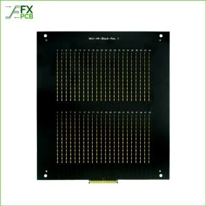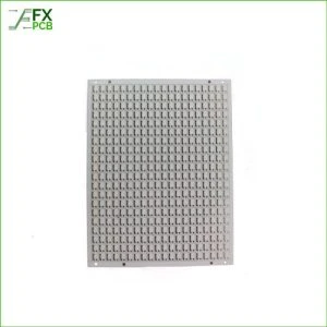
PCB panelization refers to the process of arranging multiple PCBs on a single larger board, known as a panel. By grouping multiple PCBs together, manufacturers can optimize the use of materials, increase manufacturing efficiency, and streamline the assembly process. This technique transforms the manufacturing process from producing individual boards to creating multiples in a single run, ultimately saving time and resources.

The modern-day electronics world depends heavily on the Printed Circuit Boards (PCBs) as its backbone. A PCB is a medium to transfer the current through its copper pathway and it dissipates the heat to keep the tiny yet highlycomplex electronic equipment on it in perfect condition.
If you are to get the best PCBA and PCB for your digital devices, you have to know this PCB assembly process thoroughly. FX PCB with its years of experience understands this need and thus, we present you the detailed guideline.
FX PCB dont follow the standerd manufacturing process is no exception to it. Our process includes solder pasting on the PCB base, placing the electronic components in the right place, soldering them with the PCB, checking the accuracy, final inspection, and delivery to customers.
Imagine assembling thousands of individual PCBs, each requiring separate handling and processing. It’s a nightmare of inefficiency! Panelization provides a smart solution to this challenge. Not only does it enable the simultaneous production of several PCBs, but it also simplifies the assembly and testing phases. By minimizing the manual handling of individual boards, the likelihood of errors decreases, leading to higher overall quality.
As we delve deeper into the world of PCB panelization, we’ll uncover the numerous advantages it brings to the table. From enhanced manufacturing efficiency to cost savings and improved quality control, panelization is a game-changer in the electronics manufacturing landscape. So, let’s explore these benefits in more detail.
Enhanced Manufacturing Efficiency
In the traditional manufacturing process, creating individual PCBs one by one can be time-consuming and resource-intensive. PCB panelization optimizes this process by allowing manufacturers to produce multiple PCBs in a single production run. This not only reduces production time but also minimizes the need for repeated setup and calibration, resulting in a significant boost in overall efficiency.
Cost Savings
Efficiency and cost savings go hand in hand. When PCBs are panelized, manufacturers can maximize the utilization of raw materials, reducing wastage. Additionally, economies of scale kick in, as producing multiple boards at once often leads to reduced manufacturing costs per unit. This cost-effectiveness can be a crucial factor, especially in large-scale manufacturing operations.
Improved Quality Control
Maintaining consistent quality across individual PCBs can be challenging. PCB panelization streamlines the assembly and testing processes, enabling standardized procedures. This consistency not only improves overall product quality but also simplifies the identification and rectification of any defects or issues that may arise during the manufacturing process.
When it comes to panelizing PCBs, adhering to standard panel sizes can offer several advantages. Standardization promotes compatibility with manufacturing equipment and processes, reducing the likelihood of errors during production. Commonly used panel sizes include 18″ x 24″ and 21″ x 24″, but variations exist based on regional preferences and specific manufacturing facilities.
While standard sizes offer convenience, there are instances where custom panel sizes are necessary to accommodate unique designs or specific manufacturing requirements. Customization, however, needs to strike a balance between optimizing material usage and ensuring manufacturability. Designers should collaborate closely with manufacturers to determine the most suitable panel size that meets both design and production needs.
Efficient panelization begins with strategic component placement. Proper spacing between components is crucial to prevent interference and ensure ease of assembly. A well-designed panel layout considers the optimal arrangement of components while allowing space for manufacturing and assembly processes, such as soldering and inspection.
Incorporate suitable trace and copper routing into your panel design. Maintain consistent trace widths and spacing to ensure uniform current distribution and prevent signal degradation. Design traces and copper pours with manufacturability in mind, avoiding overly intricate patterns that could lead to fabrication challenges.
The process of depanelizing individual PCBAs from a panel involves methods like V-cutting or tab-routing. V-cutting creates a perforated groove along which PCBs can be easily separated, while tab-routing involves leaving small tabs that can be broken after assembly. Careful consideration of these methods during design ensures smooth and damage-free depanelization.
Panelization impacts the assembly and soldering process. Efficient panel layouts allow for streamlined component placement and solder paste application. Components on a panel should be arranged in a way that minimizes the risk of misalignment during assembly, ensuring accurate placement and reliable solder joints.
Selecting the right depanelization method is crucial for maintaining the integrity of individual PCBs after manufacturing. Depending on the design and requirements, manufacturers can choose from various methods, including manual breaking, V-cutting machines, and routing machines. Each method has its pros and cons, so careful consideration is essential.
Successful panelization requires close collaboration between designers and PCB manufacturers. Designers should seek input from manufacturers early in the design process to ensure that the chosen panelization approach aligns with manufacturing capabilities and limitations. This collaboration minimizes design iterations and optimizes the manufacturability of the final product.
Before proceeding with mass production, thorough testing and validation of the panelized PCBs are essential. Prototyping and testing small batches help identify any design or manufacturing issues early, reducing the likelihood of costly defects in larger production runs. Rigorous testing ensures that the panelized PCBs meet quality and performance standards.

In the consumer electronics industry, where speed and cost-efficiency are crucial, panelization has become a staple practice. Smartphones, tablets, and wearable devices often employ panelization to churn out devices at a rapid pace without compromising on quality. The ability to produce multiple identical PCBs simultaneously ensures a steady supply of products to meet market demand.
Industrial electronics, such as control systems and automation equipment, often require customized designs to accommodate specific functionalities. Panelization in industrial applications allows for the consolidation of different PCBs with varying functions into a single panel. This approach simplifies assembly and reduces the chances of errors during installation, contributing to enhanced reliability in demanding environments.
As electronic devices continue to shrink in size, miniaturization presents new challenges in PCB panelization. Designers and manufacturers will need to collaborate closely to ensure that panelization methods can accommodate intricate layouts while maintaining quality and reliability. Advanced fabrication techniques and materials will play a significant role in addressing these challenges.
The evolution of manufacturing technologies, such as additive manufacturing and advanced automation, will revolutionize PCB panelization. These technologies offer increased precision and flexibility, enabling the creation of highly customized panel designs. As these technologies become more accessible, the possibilities for innovative panelization approaches will expand.
Quality assurance remains a paramount concern in PCB panelization. Robust testing and inspection procedures are essential to identify defects, such as soldering issues or faulty components, before they escalate into larger problems. Automated optical inspection (AOI) and X-ray testing are commonly used techniques to ensure the integrity of panelized PCBs.
While panelization offers numerous benefits, it also comes with inherent risks, such as the potential for stress concentration at V-cut lines or uneven solder paste distribution. To mitigate these risks, designers and manufacturers must engage in meticulous planning and validation. Additionally, choosing appropriate materials and adhering to industry standards contributes to minimizing potential issues.
Efficient panelization contributes to reduced material wastage, a critical aspect of sustainability. By optimizing panel layouts and minimizing the empty space between PCBs, manufacturers can significantly reduce the amount of scrap material generated during production. This eco-friendly approach aligns with the growing emphasis on sustainable manufacturing practices.
Incorporating eco-friendly materials and practices into panelization can further enhance sustainability. The use of lead-free solder, for instance, reduces environmental impact while complying with regulations. Designers can also explore the use of recyclable materials and consider end-of-life disposal options when designing panelized PCBs.
Insufficient clearance between components on a panel can lead to various issues, such as heat buildup, electrical interference, and difficulties during assembly. Designers must ensure adequate spacing between components to prevent these problems and facilitate efficient assembly and soldering.
Designers should always keep manufacturing constraints in mind during the panelization process. Ignoring factors like material limitations, fabrication tolerances, and assembly capabilities can result in costly revisions or even production delays. By understanding and working within these constraints, designers can create panelized PCBs that are both functional and manufacturable.
Tab routing and V-cutting are two common methods for separating individual PCBs from a panel. Tab routing involves leaving small tabs that can be manually or mechanically broken, while V-cutting creates perforated grooves for separation. The choice between these methods depends on factors like board fragility, depanelization equipment, and design requirements.
The decision to create a single panel or an array of multiple panels depends on production volume and design complexity. Single panels are suitable for low-volume production runs or prototypes, while arrays are preferred for high-volume manufacturing. Designers should consider factors like assembly line setup, testing, and shipping when making this decision.
In the ever-evolving landscape of electronics manufacturing, PCB panelization stands as a powerful technique that marries efficiency with quality. By intelligently grouping multiple PCBs on a single panel, manufacturers can streamline production, reduce costs, and ensure consistent product quality. This guide has provided a comprehensive overview of PCB panelization, from its fundamental principles to advanced best practices. As technology continues to advance, mastering the art of PCB panelization will remain a valuable skill for designers and manufacturers alike.
PCB panelization aims to optimize manufacturing efficiency by arranging multiple PCBs on a single panel, streamlining assembly processes and reducing wastage.
Can I use custom panel sizes for my PCB designs?
Yes, custom panel sizes can be used to accommodate unique designs or specific manufacturing requirements. However, designers must strike a balance between customization and manufacturability.
What are some common depanelization methods?
Common depanelization methods include manual breaking, V-cutting, and tab-routing. The choice of method depends on factors like board fragility and production volume.
How does PCB panelization contribute to sustainability?
Efficient panelization reduces material wastage and allows for the optimization of resources. Additionally, incorporating eco-friendly materials and practices enhances the sustainability of the manufacturing process.

I am Peter Gong. I have been working in PCB and PCBA industry for 15+ years now. I have been a part of the PCB revolution with my dedication to circuit board technologies and creative ideas. I write in FX PCB to impart my knowledge on PCB and PCBA for all circuit board lovers, manufacturers, and users.
WhatsApp us