PCB stands for Printed Circuit Board. PCBs have several advantages over traditional point-to-point wiring or wire-wrapping methods. They are more compact, reliable, and cost-effective, allowing for the mass production of electronic devices. They also provide a standardized platform for designing and assembling complex circuits.

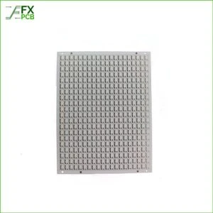
FX PCB can provide the ALN(Aluminum oxide) and AIO203(Aluminum Nitride) Ceramic PCB, we can make ENEPIG, ENIG, Immerison silver surface,you can check the material datesheet and our capability from the below tables.
The ceramic circuit board has the following characteristics: high-temperature resistance, high electrical insulation, low dielectric constant, low dielectric loss, high thermal conductivity, good chemical stability, and the thermal expansion is almost can be coefficients of components.
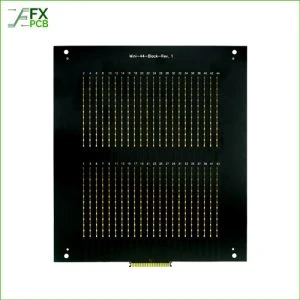
Ceramic PCB is actually made of electronic ceramic materials and can be made into various shapes. We are best Ceramic PCB Manufacturer in China
A PCB, or Printed Circuit Board, is a flat board made of non-conductive material, such as fiberglass or composite epoxy, with conductive pathways etched or printed onto its surface. It serves as a foundation for connecting and supporting electronic components in various electronic devices.
The main purpose of a PCB is to provide mechanical support and electrical connections between different electronic components, such as integrated circuits (ICs), resistors, capacitors, and connectors. These components are soldered onto the PCB, and the conductive pathways, also known as traces, facilitate the flow of electric current between them.
Design: The process begins with the design of the PCB using computer-aided design (CAD) software. The layout is created, defining the placement of components and their interconnections. The designer determines the size, shape, and number of layers for the PCB.
Fabrication: Once the PCB design is complete, the manufacturing process begins. It starts with a blank board made of the chosen non-conductive material. A layer of copper is then applied to the surface of the board. The excess copper is removed, leaving behind the desired conductive pathways according to the design layout. Holes are drilled into the board for component placement and electrical connections between layers in the case of multi-layer PCBs.
Component Placement: The electronic components, such as ICs, resistors, and capacitors, are placed onto the PCB following the design specifications. The components are typically soldered onto the board using a soldering iron or a reflow soldering process, ensuring secure electrical connections.
Routing: The conductive pathways, or traces, on the PCB allow for the flow of electric current between the components. The traces are designed to connect the various components according to the circuit’s requirements. They form a network of interconnected lines that guide the flow of electricity, ensuring the proper functioning of the circuit.
Testing: After the components are soldered and the traces are in place, the PCB undergoes testing to ensure its functionality and integrity. Electrical tests are performed to check for proper connections, shorts, and any potential defects. If any issues are detected, they can be addressed before the final product is assembled.
Integration: Once the PCB is deemed functional, it can be integrated into the electronic device it was designed for. The PCB provides the necessary electrical connections between components, allowing them to communicate and operate together as intended.
PCBs can vary in complexity, ranging from simple single-layer boards to complex multi-layer boards with multiple conductive layers. The design and manufacturing processes are crucial in ensuring the reliability and performance of the PCB and the electronic device it is used in.
The most common material used is known as FR-4 (Flame Retardant 4), which is a type of woven fiberglass cloth impregnated with epoxy resin. The core material of a PCB is usually composed of multiple layers of this substrate material, which provide mechanical support and stability to the board. The layers are laminated together to form a solid base.
The conductive pathways, or traces, on the PCB, are made of copper. Copper is an excellent conductor of electricity and is commonly used for this purpose. A thin layer of copper is applied to the surface of the PCB, either by a process called electroplating or by laminating a thin copper foil onto the substrate material.
To protect the conductive traces and provide insulation, a layer called the solder mask is applied over the copper layer. The solder mask is typically made of epoxy-based polymer or similar material and is usually green in color, although other colors such as red, blue, and black can also be used.
In addition to the core materials, PCBs may have other elements, such as solder pads, mounting holes, and silkscreen markings. Solder pads are areas of exposed copper on the board where components are soldered. Mounting holes are used for securely attaching the PCB to a chassis or enclosure. Silkscreen markings are printed on the PCB’s surface to indicate component placement, component labels, and other information.
Overall, PCBs are constructed using a combination of non-conductive substrate material, conductive copper traces, solder mask for insulation, and additional elements to facilitate component attachment and identification. This combination of materials allows for the creation of reliable and functional circuit boards.

Compactness: PCBs allow for compact circuit designs, as electronic components are mounted directly onto the board, eliminating the need for extensive wiring and bulky connections.
Easy Assembly: PCBs simplify the assembly process by providing a standardized platform for component placement. This streamlines manufacturing and reduces production time and costs.
Reliable Connections: PCBs offer consistent and reliable electrical connections between components. The use of copper traces ensures efficient signal transfer and reduces the likelihood of loose connections or signal interference.
Design Flexibility: PCBs offer design flexibility, allowing engineers to create complex circuits with multiple layers and intricate routing. This enables the integration of advanced functionalities and the miniaturization of electronic devices.
Easy Testing and Maintenance: PCBs facilitate testing and troubleshooting processes. Each component and connection can be easily accessed, making it simpler to identify and rectify faults or replace faulty components.
Cost-Effectiveness: PCBs enable mass production and automated assembly processes, leading to cost savings. The use of standardized designs and components further reduces manufacturing expenses.
Improved Signal Integrity: PCBs are designed to minimize signal loss and electromagnetic interference (EMI). Proper layout and grounding techniques help maintain signal integrity, ensuring optimal performance of the electronic circuit.
Scalability: PCBs can be scaled up or down based on the application requirements. From small, single-layer boards for basic electronics to complex, multi-layer boards for advanced devices, PCBs can accommodate a wide range of circuit complexities.
Space Efficiency: PCBs maximize the efficient use of space within electronic devices. They can be designed to fit specific form factors, allowing for space optimization and compact device designs.
Interconnectivity: PCBs enable easy integration of different electronic components and facilitate communication between them. This allows for the creation of complex systems and devices with seamless interconnectivity.
Overall, PCBAs offer numerous advantages in terms of size, reliability, flexibility, cost-effectiveness, and performance, making them a vital component in the design and production of electronic devices across various industries.

I am Peter Gong. I have been working in PCB and PCBA industry for 15+ years now. I have been a part of the PCB revolution with my dedication to circuit board technologies and creative ideas. I write in FX PCB to impart my knowledge on PCB and PCBA for all circuit board lovers, manufacturers, and users.
WhatsApp us