It is no secret that the copper coin PCB has changed the world of the electric device with its groundbreaking technology. From the largest electronic device to the smallest one, every electrical equipment has leaped with the use of Printed Circuit Boards.
But when did it first started and where the future of printed circuit board is heading towards? Also, what about the latest embedded copper coin PCB?
For our valued customers and readers, we are going to shed light on the history, manufacturing process, and uses of PCB copper coins.
Are you up for it?
Table of Contents
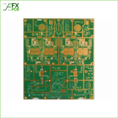
Our Recommended Copper Coin PCB
Copper base PCBs are the most demanding and expensive of all the three types of printed circuit boards. It got the name because the circuit board substrate is made of copper. The use of copper makes these circuit boards highly thermally conductive and versatile.
The copper foil used as the substrate typically has a thickness of around 35μm~280μm. Its thermal conductivity is further assured with the use of aluminum oxide and silicon powder. The manufacturer also usesepoxy resin to connect the substrate and the leading copper circuit.
The epoxy resins are often filled with polymer for the secured connections.
What Is Copper Coin PCB?
A basic PCB comes with a layer of high-quality copper foil that covers the insulating material with a substrate. It provides mechanical support, and then effortlessly connects the electronic components. It mainly used electrically conductive pads or tracks to connect the electronic components securely.
Initially, PCB copper coins were used for regular heat dissipation. However, with the advancement of electronics and the emergence of tiny electronic circuits, the industry needed even higher heat dissipation capacity in the PCB. This lead to the rise of embedded copper coin PCB. It has higher thermal conductivity and so, disperses the heat faster than regularly printed circuit boards.
The History of PCB Copper Coin
As far as the PCB copper coin manufacturers are concerned, the history dates back to the early 20th century. Since then, it has gone through immense change that has changed the world technology itself with outstanding contributions to the electric and electronic arena.
The First Impression
Albert Hanson, the German electric legend, first patented the PCB at the beginning of the 20th century. However, due to the 1930’s world economic recession, Hanson’s dream of manufacturing PCB in the industrial-scale was delayed to 1943.
In 1943, the US army started using the PCB is making proximity fuses. Later, Paul Eisler developed the PCB to the next level of use.
The Spreading of Technology
For the next three decades, PCB spread worldwide from the USA to their rival Soviet Union. During the 1905’s US army started mass production of the PCB. It helped the electronics consumers use the PCB at the mass level.
The next breakthrough came from Hazeltine Corporation, which used through-hole plated™ technology. It helped them to use the PCB copper coin without the crossover connection.
The Emergence of Integrated Circuit
The birth of IC or Integrated Circuit came into being in the early 1970s that boosted the printed circuit board technology to another groundbreaking level. Although the first IC was invented way back in the ’50s, it took almost 20 years to be sued widely in the electronics world.
The emergence of IC meant that nothing now can be done without the PCB. They became an integral part of each other.
Updating the PCB Design
During the 1980s, PCB copper coin manufacturers took another big leap towards the PCB design. Until then, the printed circuit board was design at hand. Thus, it was to be made on a large scale, and design transportation was only possible through photographs.
At this time, with the advancement of computer technology, Electronic Design Automation, or EDA developed quite rapidly. It permitted engineers to design the PCB in software. It made the whole system dynamic and helped in scaling down the PCB size.
So, during this time, we see the rapid development of cellphones and Walkman, who were benefitted by the updated PCB design.
Towards the Journey of Ultra-Lightweight PCB
By this time internet had been making revolutions worldwide, and desktop computers were spreading like a fire everywhere. It meant that the manually designed PCB is no more compatible with being used in the electronic.
So, it was clear that the era of automated PCB has started. Hence, embedded copper coin PCB suppliers started the mad race of making the lightest and smallest PCBs. At this time, engineers and PCB builders also focused on building versatile PCBs that can later be developed and fixed for further usage.
Multiplicity Prevailed:
Finally, the PCB entered the 21st century, and at the same time, the age of multiplicity for PCBs also emerged. Builders were concerned about making PCBs that can perform multiple tasks simultaneously, which even a decade ago was thought impossible.
And the difference is seen in today’s home appliances. A TV can now surf the internet and showcase videos from your smartphone. Moreover, a smartphone is almost performing like a desktop PC.
With such advancement, what’s the future of PCB? Well, only the future knows it.
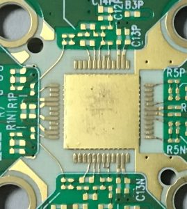
Use and Characteristics of Embedded Copper Coin PCB:
Where high heat dissipation is essential, only a PCB cannot perform the task. High heat dissipation within a quick time requires the insertion of an embedded copper coin so that it becomes fast and reliable. That’s why the PCB with copper coin emerged into the electronic world.
It has some pretty distinctive features-
- High-speed connectivity between multiple circuits.
- Its high thermal conductivity means it can transport heat better and evenly.
- The copper coin for PCB also ensures high heat dissipation with better control and even distribution.
These updated features have made possible the use of embedded PCBs into today’s various projects. These include-
- 5G network connectivity
- Modern-day electronic cars
- High-power in a small battery
- Audio productivity.
Frequently Asked Questions (FAQ) About Copper Coin PCBs
Q1: Copper Coin vs. Thermal Vias: Which is better?
A: While thermal vias are cost-effective, Copper Coin PCBs offer far superior thermal conductivity. A solid copper coin can reach a conductivity of approximately 380-400 W/mK, whereas thermal vias (filled with air or solder) are limited by the thermal resistance of the dielectric and plating, making copper coins the “best” choice for high-heat applications like 5G and EV electronics.
Q2: What are the different types of Copper Coin designs?
A: There are three main types:
Embedded Copper Coin: The coin is pressed into a pre-milled cavity after the lamination process.
Buried Copper Coin: The coin is integrated during the lamination of the inner layers.
Press-fit/U-Coin: Specifically shaped coins designed to fit complex component geometries for maximum surface contact.
Q3: Does using a Copper Coin PCB significantly increase the cost?
A: Yes, the manufacturing process is more complex, involving precise CNC milling and specialized bonding. However, it often reduces overall system costs by eliminating the need for bulky external heatsinks or active cooling fans.
Q4: What are the key considerations for Copper Coin PCB design?
A: Designers must pay close attention to the CTE (Coefficient of Thermal Expansion) mismatch between the copper and the FR4 substrate. Proper clearance and tolerance settings in your Gerber files are essential to ensure structural integrity during soldering and thermal cycling.
Conclusion
Since the invention in the early 20th century, PCB has seen some immense and unthinkable development. And in this regard, copper coin PCB has come a long way from being a simple circuit to a multilayer and multi-dynamic electronic circuit board capable of performing numerous tasks at a time.
However, you need to ensure that you get the cooper coin for PCBV from a trusted supplier to ensure quality and reliability. Once you can assure it, the electronics device manufacturing will be a breeze work to you.

One Response
Nice article. Would have been more useful if you could include a brief list of leading embedder copper coin pcb suppliers