Printed circuit boards have huge applications in almost every industry. To execute a successful electronic project, you need skilled pcb manufacturing company. In this article we are going to teach you everything you need to know about printed circuit boards. Don’t miss it!
What is a printed circuit board or PCB?
So that you understand from the beginning what a PCB is, it is what makes all the electronic devices around you work. For example, the computer or mobile you are using to read this article has a PCB that makes it possible to perform all the actions you want. Moreover, printed circuit boards can be considered the “organs” of electronic devices.
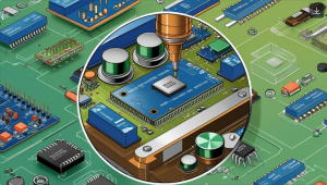
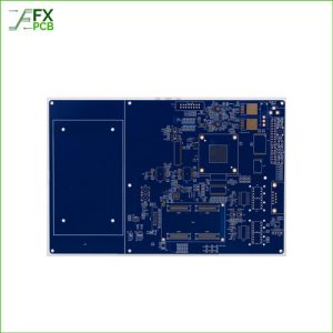
If we get more technical, a PCB is a physical support in which we install different electronic or electrical components that interconnect with each other, such as resistors, capacitors, chips, and connectors…
If you have the opportunity and look inside a computer you will be able to see several flat plates, these are motherboards that have a PCB and the components that we mentioned above attached to them.
For the energy to pass between them, through very fine conductive tracks, generally made of copper, a rail is generated that performs a function similar to that of a cable.
We can find both a simple plate that can have conductive tracks on one side and both and more complex ones that have these tracks stacked in multiple layers.
To support these tracks and the components in them, a combination of ceramic materials, resins… with fiberglass is used. Although thanks to today’s advances, we can find materials such as celluloid or conductive paint tracks.
Historical background of the printed circuit board
The inventor of the printed circuit is believed to have been an Austrian engineer named Paul Eisler around the year 1936, when he made a radio.
In the year 1943, approximately, they began to manufacture radios on a large scale for use in the Second World War, and when it ended, the United States released the invention so that it could be commercialized. But it was not until the 1950s that they became popular. Similarly, in these years, the US Navy developed self-assembly.
Before the creation of printed circuits, the point-to-point connection was carried out and for small productions or prototypes, the wire wrap method.
The first printed circuits that were created are not like those of today. Originally, electronic components were used as copper or brass pins. Furthermore, these were several millimeters long, and holes for these pins were drilled into the circuit.
These components were soldered to the board and passed through the holes. Moreover, this method was called through the hole.
In 1950, as we have mentioned, self-assembly was created. This method consisted of component pins being inserted into the interconnect pattern foil and subsequently soldered.
Finally, with advances in card lamination and engraving techniques, this process evolved into what is done today. The soldering is done automatically through a flow of molten solder, in a wave soldering machine.
Furthermore, the cost that was associated with the holes that had to be made disappears thanks to surface mounting.
What is inside a printed circuit board?
The most complex circuits are made up of several conductive layers, separated by a substrate, an insulating material.
To connect the tracks of different layers, holes called vias are used that may or may not go completely through the PCB.
It is important that, although the substrate may have different compositions, none of these are conductive. Each electrical track has its own signal and voltage. Two types of substrates are commonly used. Pertinax and FR-4, a resin-coated fiberglass materials that are fire-resistant.
When we talk about electronic components, they will go on the outside of the PCB and normally on both sides.
PCB board creation process
We have already been able to learn that they are made up of integrated circuit boards, but below, we will list the steps to manufacture a PCB:
- PCB design using software
- Serigraphed and photographic tracing
- Printing of inner layers
- Inspection and verification (AOI)
- Oxide film and lamination
- Drilling holes
- Metallic drilling
- Outside film of tracks and electroplating
- Strip etch strip
- Welding mask and legend
- Soldering of components and final tests.
If you want to know more curiosities about electronics, stay tuned to our blog and our social networks.
Where to get the best pcb manufacturing services in China?
The best website to get pcb board manufacturing and pcb assembly is Fx pcb.