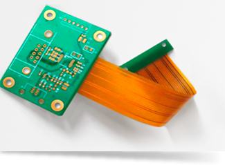
Exploring the Advantages and Cost Considerations of Rigid-Flex PCBs
SFX PCB works with ceramic PCB and varieties of PCB products. So, we have decided to share the definition and its uses with our readers. Ceramic PCB is a circuit board made with a ceramic base material.
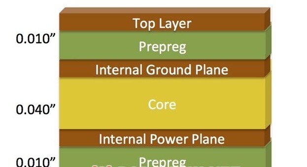
Ultimate Guide to PCB Copper Thickness and 4-Layer PCB Stackup in Panel Design
SFX PCB works with ceramic PCB and varieties of PCB products. So, we have decided to share the definition and its uses with our readers. Ceramic PCB is a circuit board made with a ceramic base material.
Complete Guide to the Manufacturing Process of Ceramic PCB
SFX PCB works with ceramic PCB and varieties of PCB products. So, we have decided to share the definition and its uses with our readers. Ceramic PCB is a circuit board made with a ceramic base material.
PCB vs PCBA – What’s the Difference

SFX PCB works with ceramic PCB and varieties of PCB products. So, we have decided to share the definition and its uses with our readers. Ceramic PCB is a circuit board made with a ceramic base material.
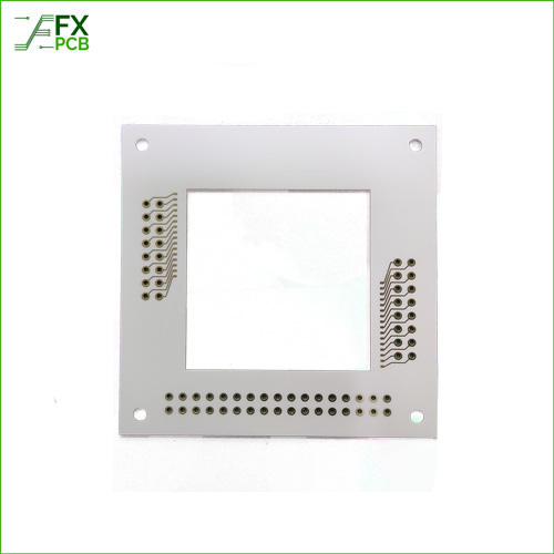
Ceramic PCB: Its Materials, Types, Benefits and Drawbacks

SFX PCB works with ceramic PCB and varieties of PCB products. So, we have decided to share the definition and its uses with our readers. Ceramic PCB is a circuit board made with a ceramic base material.
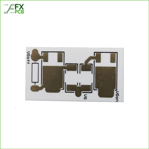
Ceramic PCB: A Detailed Material Property Comparison
SFX PCB works with ceramic PCB and varieties of PCB products. So, we have decided to share the definition and its uses with our readers. Ceramic PCB is a circuit board made with a ceramic base material.
Advanced Soldering Materials for PCB Assembly

SFX PCB works with ceramic PCB and varieties of PCB products. So, we have decided to share the definition and its uses with our readers. Ceramic PCB is a circuit board made with a ceramic base material.
Introduction of the Ceramic PCB Manufacturing Process
SFX PCB works with ceramic PCB and varieties of PCB products. So, we have decided to share the definition and its uses with our readers. Ceramic PCB is a circuit board made with a ceramic base material.
Surface Mount Technology vs Through-Hole Technology

SFX PCB works with ceramic PCB and varieties of PCB products. So, we have decided to share the definition and its uses with our readers. Ceramic PCB is a circuit board made with a ceramic base material.
The Advantages of Outsourcing PCBA Manufacturing
SFX PCB works with ceramic PCB and varieties of PCB products. So, we have decided to share the definition and its uses with our readers. Ceramic PCB is a circuit board made with a ceramic base material.