Today, we will discuss the meaning of double-sided PCB boards, their uses in different sectors, and their benefits. The discussion also includes the essential difference between single and double-sided PCBs. If you are genuinely enthusiastic to know more about double-sided PCBs, read the article.
What Is A Double-Sided PCB Board?
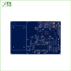
Double-sided printed circuit boards, unlike their cousin, single-sided PCBs, have conductive layers on either side of the board. So, you will find circuit traces on both sides of these boards. Manufacturers will use plated holes to connect the two sides.
With double-sided construction, these PCBs require complexity for many high-end electronic devices. There will also be copper circuit layers that surround the dielectric layer. Also, both sides have solder masks as a finished product.
The boards and holes of the double-sided PCBs may have different materials. SFX FCB, with more than ten years of experience in circuit board manufacturing, offers you different types of double-layer PCBs. Whether you need these PCBs for beginner or intermediate-level appliances and devices, SFX PCB is ready to provide you with the most affordable double-layer PCBs.
As the component and conductive layer of copper are found on both sides, the traces can cross over. It allows the circuit boards to work with more electricity without being too heated. So, the double-sided PCBs increase the productivity and efficiency of electrical and electronic devices. Using them in high-end devices will ensure long-lasting and reliable performance at an affordable cost.
Double-Sided PCB Manufacturing Process
Double-sided printed circuit boards may look complex, but their manufacturing process is not so complex. At SFX PCB, we ensure the most streamlined and advanced PCB manufacturing process for the 2 Layer PCB. It enables us to maintain the best quality and deliver the best performance for the circuit boards.
We only guarantee to make and deliver the best dual-sided PCBs at SFX PCB. To better understand how our dual-layered PCBs are more efficient and dependable, we will discuss their actual manufacturing process.
Designing and printing the layouts:
We will first design the layout of the PCBs using the designing software. Our expert engineers will use OrCAD, Eagle, and Proteus software to design the layout of the double-sided PCBs’ top and bottom parts. As we use the most advanced designing software for PCB layouts, it ensures exceptional design. So, we can follow your necessity and business demands for PCBs.
Once our designers have finalized the layout, we will print it. We use high-glossy and quality paper to print the circuit board layouts. Since we use quality glossy paper and enlarge the design, we can look into it closely to find any errors.
When we find any error or any place for improvement, we will quickly fix it. Then, our primary manufacturing process will begin.
Applying the design on the copper substrate:
Now, it’s time to print the layout on the copper substrate. We will use copper fiberglass as the substrate material for the double-sided PCBs. In the first end, copper is an excellent medium to dissipate heat and conduct electricity. On the other hand, fiberglass is easy to work with and sturdier than most materials. So, you can enjoy peace of mind knowing that the fiberglass and copper substrate ensure better and improved device longevity.
Now, let’s get back to the manufacturing steps.
- Once we have outsourced the copper fiberglass base, we test it for defects. Also, we will remove any impurities from the substrate using various chemical applications.
- After removing the defects from the fiberglass-plated copper, we will work on it. At this step, we will cut the substrate according to the size requirement of the PCBs. Our expert workers will use CNC cutting machine to cut the substrate accurately.
- At this moment, the Cloth Iron needs to be set at max temperature. So, it will imprint the layout on the copper base. Printing the layout on the copper base using the Cloth Iron takes 20 to 30 seconds. It leaves a laser ink trace on the base.
- With a scrubber, we will remove the trace of the laser ink from the copper base. It needs multiple scrubbing with added caution, so it doesn’t wash out the main PCB layout.
- Now, it’s time to repeat the substrate cleaning and PCB design printing on the other side of the base. It also needs to be appropriately cleaned so there are no chemical defects or impurities. Or else the base won’t work correctly.
It needs special attention as engineers work with the fiberglass and copper base and print the layout using Cloth Iron. It is necessary to ensure that the layout is aligned accurately on both sides of the PCBs. Or else the circuit board will be in vain.
Drilling the holes and etching out the copper:
After applying the layouts over the double-sided printed circuit boards, engineers will drill the holes. It allows the circuit board to have proper alignment and connectivity. Our experts use high-end cutting machines to cut and drill the holes as accurately as possible.
Once the holes are drilled, we must etch out the substrate’s copper. It will allow the printed circuit boards to work brilliantly without any flaws. We will put the layout printed circuit boards on the CuCl3 or FeCl3. The copper chloride solution needs to work for 20 to 30 minutes over the circuit boards to etch out the copper. So, the copper base and PCB layout will be flawless and ensure better performance.
Making the PCBs conductive:
Before soldering the components to the circuit board, we must make it conductive. It helps us to maintain proper electricity and heat conductivity and ensure brilliant performance. For this, we will use a conductive pen and ink. The tip of the conductive pen needs to be refined to provide the circuit boards with the most accurate design.
It makes the PCBs perfect with the plated through or conductive holes. As you use the conductive pen, ensure to use the finest tip. It yields better inking results.
Soldering of the double-sided PCBs:
Our PCBs are almost ready at this stage, except for the soldering part. So, it’s time we start soldering the PCBs with the components. First, we will apply the green solder mask over the double-sided circuit boards. The green soldering will be over both sides of the PCBs.
Now, it’s time to solder the components on the double-sided PCBs to complete the assembly process. This way, we complete the double-sided PCBA system with gr success and performance.
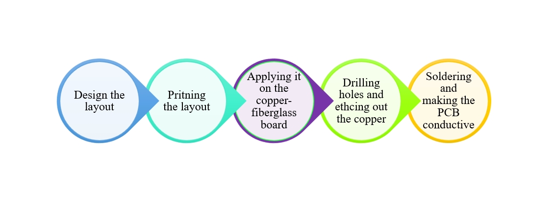
Figure 1: The manufacturing process of double-sided PCBs
The diagram should help you quickly understand the double-sided PCB manufacturing process as SFX PCB follows.
Double-Sided PCB VS Single-sided PCB
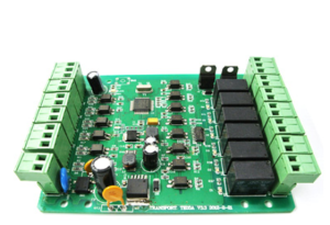
Double-sided PCBs offer numerous benefits compared to single-sided PCBs including increased circuit density, compact design, reduced manufacturing costs, and the ability to source and sink current. They are used in a wide range of applications such as power supplies, HVAC systems, LED lighting, car dashboards, and more. At SFX PCB, you can obtain high-quality double-sided PCBs at affordable prices and with fast delivery for both prototypes and mass orders. Contact our experts for any inquiries about double-sided PCBs and their assembly.
The printed circuit board sector has continuously gone through development. As a result, it has presented us with many different types of PCBs. Double-sided PCB is one of them. It is a successor of single-sided PCBs. While single-sided PCBs have a conductive surface only, double-sided printed circuit boards will have a conductive layer on each side. So, it comprises two layers of conductive surface. There will be a copper layer and solder masking too.
The conductive copper layer will be on both sides of the base. Manufacturers will apply Vias to create the traces on the conductive copper layer. You can securely connect the different components on both sides of the base with the Vias. It improves both the security and performance of the double-sided PCBs.
The main difference between the double and single-side PCBs are listed below:
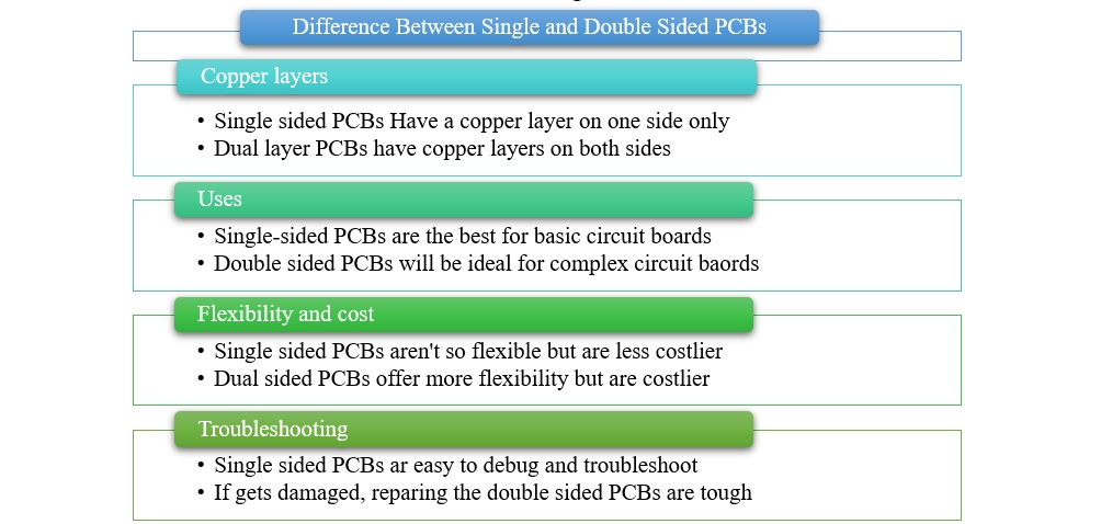
Figure 2: Difference between double and single-sided PCBs
As you see the difference between the double and single-sided PCBs, you should now know which PCB to apply where. Usually, double-sided PCBs are made for complex devices with more longevity. Although costlier, SFX PCB has streamlined the design and manufacturing process. So, we can offer you the cheapest double-sided PCBs without compromising quality.
Benefits of Using Double-Sided Printed Circuit Boards:
Double-sided printed circuit boards have revolutionized the circuit, electronics, and device market. But what makes these circuit boards so beneficial? What are the advantages of using these circuit boards over conventional ones?
- Double-sided layers have copper traces on both sides. So you will have more space to attach the components. This way, you can solder more components on the double-sided PCBs. It improves the circuit density making it ideal for complex uses.
- Since double-sided PCBs have more circuity density and are more complex, they are used in making complex devices. So, home appliances and daily device manufacturing costs are considerably reduced. People can, therefore, get them at affordable pricing.
- The compact design of these PCBs has reasonably reduced the devices’ size. It has enabled manufacturers to make their devices more potent without making them too large. As a result, home appliances and industrial devices now fit into more compact spaces. It also makes device maintenance effortless.
- These PCBs have reduced the cost of manufacturing devices reasonably. You can expand the design and components on the same copper surface without effort. Therefore, it allows you to cut costs and still make high-end devices. As it has copper traces on both sides, you don’t need to add multiple layers. Naturally, the cost reduces.
- Lastly, you can use the double-sided printed circuit boards for sourcing current. You may even use them for sinking purposes. The bottom layer is usable as the ground copper base. It can sink and source current, and the top layer will remain free. So, you can redirect the current using the bottom layer and keep the top side free for components and the soldering process.
As you see, double-sided printed circuit boards bring myriad benefits in real life. If you wish to maximize your profit and enjoy better longevity of the devices.
Applications of Double-Sided PCBs:
We have mentioned multiple times that dual-sided PCBs have changed the direction of the electrical and electronics industry forever. So, you will see its applications in different sectors. Its critical applications include:
- Power supplies
- HVAC systems
- Power conversion
- Hard drives
- Phone systems
- Traffic systems
- Car dashboards
- LED lighting
- Printers
- Vending machines
Conclusion
Double-sided printed circuit boards are so beneficial that they will give you a wow factor. And at SFX PCB, you can get the best double-sided PCBs at the most reasonable pricing. We provide mass orders faster to meet your device manufacturing demands. Whether you need a prototype or bulk amounts of finished PCBs, we will provide you with them. You can reach us anytime; our experts will respond faster than you imagine.
Henceforth, you will get accurate double-sided PCBs and kick off your device and home appliance business big time. You can reach us for any queries on any printed circuit board and its assembly as well.