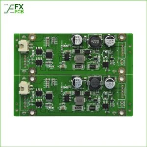
This may seem a wild idea, but you can indeed manufacture circuit boards at home. Yes, the process may seem tough initially, but you love when you finish the circuit board manufacturing. The real question is how to etch a circuit board.
Well, we have solved this issue for you. Yes, today, we will guide you through the steps to etch a circuit board at home. The etching of the circuit board means drawing the design on the copper base to find the actual diagram.
We have simplified the circuit board etching process to make it easy for you, even if you are going to try it for the 1st time.
So, without spending much time, let’s dive deep into the circuit board etching process. Aren’t you excited?
When you decide to prepare a circuit board at home, you must maintain its accuracy with the right diagram. It is crucial since the circuit board holds multiple electric components linked to durability with electricity. Any flaws in the circuit board design will lead to the death of the device immaturely.
The etching process includes the following steps-
Since you will work with electricity and highly complex components in demanding conditions, you must never ignore safety. Therefore, we recommend you wear goggles and gloves. It will protect your hands from unnecessary cuts and eyes from any flying objects. Furthermore, the etching solution is a skin irritant which makes wearing gloves even more important.
Also, use surgical gloves to work with the circuit board copper base. It will allow you to work with improved accessibility and comfort with the copper substrate.
The chemicals and mixing solution used in etching the circuit board are often high in fume and smoke. It can suffocate you, especially if you work in a crowded place. Hence, make sure you work in a well-ventilated space with proper lighting.
To etch the design on the copper plate for preparing the circuit board, you will need to print it on paper. You can get the design from the following suppliers-
These manufacturers offer free design. Or, if you have time and skills, you can always work on Adobe Illustrator to prepare your design. But it can be tedious since you have to know precisely where to put which component.
Also, you need to use transfer paper to print the circuit board design. Before you print out the circuit board design, don’t forget to flit it. Otherwise, you will end up getting the wrong direction for the diagram.
From this point, you will work with the etching solution and copper plate. So, start the suggested surgical gloves from here. On one side, it protects your hands from the harmful etching chemical and saves the copper plate from any oiling.
Use fine-grip sandpaper to sand off the copper plate. Also, sand the edges with better precision. It removes any debris and provides a smoother surface better for etching. Lastly, use rubbing alcohol and water to wash off the plate. You may even use nailpolish remover instead of rubbing alcohol.
You will require a laminator during this process. Put the design down facing the copper plate. You will need to pass it through the laminator five to seven times at least. You have to continue passing the design and copper plate through the laminator until it becomes hot.
You may even use an iron instead of a laminator. The use of iron is preferable for home use since most homes may lack a laminator.
Now you will need to prepare the etching solution. The aim is to rinse off the remaining copper from the plate and leave the design only. You will need-
You need to prepare enough solution to submerge the laminated copper plate in it. Also, remember that the mixed solution will release chlorine gas. So, it is toxic and highly skin irritant. Moreover, it would be best to prepare the solution in a plastic container to avoid misspells and damage.
Now, submerge the copper plate made circuit board in the solution. Agitate the circuit board gently for the next 1- to 15 minutes roughly.
Keep your face away since the solution will produce a fume as it gets warmer during the agitation process. Or it may burn your face. Hence, be careful.
You will need to continue the hydrogen peroxide and hydrochloric acid solution for some more minutes. You must stir it until the copper on the circuit board has completely dissolved. It is essential for a flawless design.
The solution will turn into more of a green tinge as you stir it to dissolve the copper. Never take off your goggles and gloves during the entire process.
Run cold water from the water spout. Place the board under it the running water as you wear gloves. Make sure you have cleaned off the entire etching solution from the copper board. Now, use a clean rag to wash and dry off the board.
In a separate bowl, mix one part of acetone with one part of rubbing alcohol. Use a towel to wash off the board with the cleaning solution. Dip the towel in the solution and rub it on the board gently. As you continue rubbing the solution-mixed towel on the board, it will slowly remove the marker from the inscribed board.
When you continue rubbing the mixture on the copper board, you will soon get the circuit board design inscribed on it. Use a clean rag to wipe off any remaining solution, and the circuit board design will be ready for use.
Etching a circuit board at home isn’t as difficult as it seems. This guideline on how to etch circuit boards at home should make the process easier for you. The only concern of you is maintaining proper safety features since the solution used to etch the copper board will be highly toxic.
Hence, you have to dispose of the solution properly. You must use a good plastic bottle to collect the remaining solution. For the dumping, label it ‘Chemical wastage.’ Also, you can add hydrogen peroxide to it and store it for future use.

I am Peter Gong. I have been working in PCB and PCBA industry for 15+ years now. I have been a part of the PCB revolution with my dedication to circuit board technologies and creative ideas. I write in FX PCB to impart my knowledge on PCB and PCBA for all circuit board lovers, manufacturers, and users.
WhatsApp us