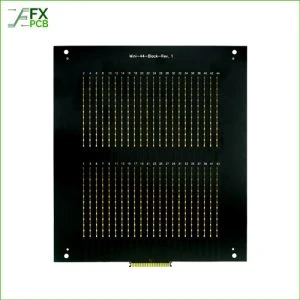
Gerber files are the de facto standard in the PCB manufacturing industry for conveying design information to fabricators. They serve as a universal language that communicates the intricacies of your PCB design, including the placement of components, traces, pads, and more. Think of Gerber files as the blueprint of your design, providing manufacturers with precise instructions to bring your creation to life.

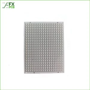
Light PCB assembly is the process of assembling and soldering electronic components onto a printed circuit board (PCB) to form a functional electronic device. The PCB material should be chosen based on factors like fire retardant, dielectric constant, loss factor, tensile stability, glass transition temperature, and Z-axis expansion coefficient. Common materials used for Light PCBs are CEM-1, CEM-3, FR-4, aluminum, and copper alloys. The material should be selected based on the specific requirements of the electronic device being produced.
Shenzhen PCB assembly manufacturer is the ideal place for your Light PCB assembly needs. We can assist you in assembling everything from industrial high-power LEDs to commercial flood LEDs.
While Gerber files capture the essence of your design, the board size plays a pivotal role in determining the physical dimensions and spatial layout of your PCB. A well-chosen board size can optimize functionality, manufacturability, and even cost-effectiveness. It’s essential to recognize the interplay between Gerber files board size to achieve a harmonious and successful PCB design.
Gerber files consist of multiple layers, each representing a specific aspect of your PCB design. These layers include the top and bottom copper traces, solder mask, silkscreen, drill holes, and more. Each layer is like a slice of your design, contributing to the overall complexity and functionality of the PCB.
At a granular level, a Gerber file is composed of commands that instruct the manufacturing equipment on how to create each layer of the PCB. These commands are like the building blocks of your design, dictating actions such as drawing traces, placing vias, and defining component outlines.
Modern PCB design software plays a crucial role in generating accurate and comprehensive Gerber files. These software tools allow designers to create intricate designs, complete with multiple layers, components, and precise dimensions. When it comes to exporting Gerber files, the software compiles all the design data into a format that fabricators can readily understand and use.
Generating Gerber Files: Step-by-Step
Design Completion: Finalize your PCB design, ensuring that all components, traces, and layers are in place.
Layer Configuration: Configure the different layers of your design, specifying attributes such as copper thickness and solder mask.
Export Settings: Choose the appropriate export settings in your PCB design software. Select the layers to be included in the Gerber files.
File Generation: Initiate the export process, allowing the software to compile and generate the Gerber files.
Verification: Before sending the Gerber files to the manufacturer, conduct a thorough review to ensure accuracy and completeness.
The dimensions of your PCB can significantly impact its performance and functionality. Standard board sizes are often defined by industry conventions and form factors, such as the popular ATX and Mini-ITX sizes. However, these standards are not set in stone, and designers have the flexibility to customize board dimensions to suit their specific needs.
The gerber files board size directly influences factors like signal integrity, thermal management, and ease of assembly. A larger board allows for more components and complex designs, but it might come at the cost of increased manufacturing complexity and expenses. Conversely, a smaller board may prioritize miniaturization but could pose challenges in terms of routing and heat dissipation.
When designing PCBs for wearable devices, such as smartwatches or fitness trackers, miniaturization is a primary consideration. The compact size of these devices demands creative and efficient utilization of board space. Gerber files play a crucial role in ensuring that components are placed optimally to achieve a sleek and functional wearable design.
In contrast, industrial applications often require larger PCBs to accommodate intricate control systems, power electronics, and extensive connectivity options. Board size optimization in these scenarios involves striking a balance between housing all necessary components while adhering to spatial constraints within machinery or equipment.
Gerber files encode design data through a series of commands and coordinates. These commands dictate the placement of traces, pads, vias, and other design elements. The precise coordination of these components within the Gerber files ensures that the physical board matches the intended design.
Whether your design calls for a compact PCBA or a sprawling one, Gerber files remain adaptable. Designers can leverage the flexibility of Gerber files to adjust the placement and configuration of components based on the chosen gerber files board size. This adaptability underscores the versatility of Gerber files in accommodating diverse design requirements.

A common pitfall in PCB design is overcrowding the board with components, traces, and vias. While maximizing space is crucial, an overly congested design can lead to signal interference, heat buildup, and manufacturing challenges. Striking a balance between efficient space utilization and design clarity is essential.
Incorrectly sizing the PCB can lead to a cascade of issues, from manufacturing defects to performance degradation. Oversized boards might result in wasted space and increased material costs, while undersized boards could hinder proper component placement and compromise functionality. Thoroughly evaluating and validating board size decisions is imperative.
Design for Manufacturing (DFM) principles are paramount to ensuring smooth and cost-effective production. When preparing Gerber files, adhere to DFM guidelines that accommodate the manufacturer’s capabilities and processes. This includes considerations for trace widths, spacing, solder mask, and other critical design aspects.
Effective communication with your chosen manufacturer can yield significant benefits. Engage in discussions about board size requirements, material options, and manufacturing constraints. By collaborating closely, you can fine-tune your Gerber files and optimize the board size to align with the manufacturer’s capabilities.
Prototyping is a crucial phase in PCB design, allowing you to validate your concept and identify potential issues before mass production. Gerber files serve as the foundation for prototyping, enabling manufacturers to create accurate prototypes that mirror the final product’s form and functionality.
Prototyping with Gerber files provides the opportunity for iterative testing and refinement. By observing the performance of the prototype, you can make informed adjustments to the board size and component placement. This iterative process enhances the quality and reliability of the final PCB design.
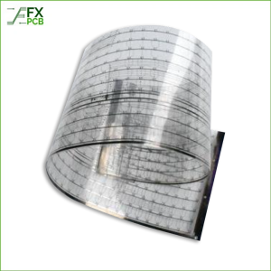
The landscape of PCB design is evolving, with a growing emphasis on flexible PCBs and custom form factors. These innovative designs often require unique gerber file board size and configurations to accommodate bending, folding, or unconventional shapes. Gerber files play a crucial role in translating these intricate designs into tangible, functional PCBs.
As technology continues to advance, miniaturization remains a driving force in PCB design. Smaller, more compact devices are in high demand, pushing designers to push the boundaries of what’s possible within limited board space. Gerber files will continue to be instrumental in achieving the delicate balance between miniaturization and performance.
In a rapidly changing technological landscape, designing for scalability and adaptability is paramount. Gerber files provide a solid foundation for future-proofing your designs. By creating Gerber files that can be easily adjusted and modified, you ensure that your PCB designs can accommodate future upgrades and changes.
Anticipating potential design changes is a proactive approach to PCB design. Whether it’s the addition of new components or changes in functionality, Gerber files can be adjusted to accommodate these alterations. By incorporating flexibility into your Gerber files, you empower yourself to respond effectively to evolving design requirements.
Mastering the intricate dance between Gerber files board size is a hallmark of successful PCB design. As you embark on your design journey, remember that Gerber files are more than lines of code—they are the conduit through which your creative vision becomes a tangible reality. With careful consideration of board size, adherence to industry best practices, and a touch of design ingenuity, you can craft PCBs that not only meet specifications but also exceed expectations.
Absolutely not! While Gerber files are the most widely used format, other formats like ODB++ and IPC-2581 also serve similar purposes in conveying design data to manufacturers.
Yes, you can adjust the board size after generating Gerber files, but it may require modifications to other design elements to maintain proper functionality and manufacturability.
Panelization involves grouping multiple PCB designs onto a single larger panel for manufacturing efficiency. It can impact board size considerations and production costs.
While it’s technically possible to prototype a PCB without Gerber files, using Gerber files ensures accurate representation of your design and facilitates smoother prototyping and manufacturing processes.
Choosing the right manufacturer involves evaluating their capabilities, experience, and compatibility with your design requirements. Engage in open communication and request samples or references before making a decision.

I am Peter Gong. I have been working in PCB and PCBA industry for 15+ years now. I have been a part of the PCB revolution with my dedication to circuit board technologies and creative ideas. I write in FX PCB to impart my knowledge on PCB and PCBA for all circuit board lovers, manufacturers, and users.
WhatsApp us