The world of electronics manufacturing is fast-paced, evolving, and intricate. Among others, ceramic Printed Circuit Boards have emerged as a cutting-edge solution.
A Ceramic PCB Manufacturer provides unique solutions, effectively addressing the increasing demands for higher performance, longer lifespan, and enhanced thermal management. This article delves into the fascinating world of ceramic PCB manufacturing, outlining this technological marvel’s process, benefits, and applications.

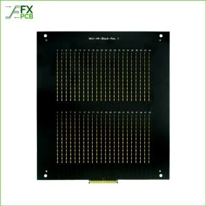
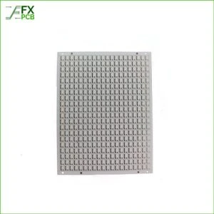
FX PCB can provide the ALN(Aluminum oxide) and AIO203(Aluminum Nitride) Ceramic PCB, we can make ENEPIG, ENIG, Immerison silver surface,you can check the material datesheet and our capability from the below tables.
The ceramic circuit board has the following characteristics: high-temperature resistance, high electrical insulation, low dielectric constant, low dielectric loss, high thermal conductivity, good chemical stability, and the thermal expansion is almost can be coefficients of components.
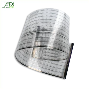
Ceramic PCB is actually made of electronic ceramic materials and can be made into various shapes.
Traditionally, PCBs were made of materials like FR4 or CEM, types of fiberglass that are affordable but have limitations regarding heat dissipation, thermal expansion, and frequency performance. These shortcomings became pronounced with the miniaturization trend and higher operating frequencies, pushing manufacturers towards more suitable materials; Ceramics.
Ceramics, known for their exceptional thermal conductivity, electrical insulation, and chemical stability, offer a promising alternative for manufacturing PCBs. Suitable for high-power applications of electronics, they are durable at high temperatures and probably the most common reason for being a common alternative to standard FR4 boards. But how are ceramic PCBs manufactured? Let’s find out.
The first step in the ceramic PCB manufacturing process involves creating the ceramic substrate. High-purity alumina or aluminum nitride powders are the primary materials used. They are mixed with organic binders and solvents to create a viscous paste. This paste is then subjected to tape casting or a similar technique to produce a thin sheet.
Following this, the ceramic sheet undergoes a process known as debinding. Here, the organic materials are slowly removed by heating, leaving behind a porous ceramic body. Finally, the substrate is sintered in a kiln at high temperatures, resulting in a dense, robust ceramic plate ready for the next stage.
In the fascinating journey of ceramic PCB manufacturing, the process of metalization comes across as a significant milestone. Think of it as creating a conductive roadmap on the blank canvas of the ceramic substrate.
Picture an artist carefully creating a masterpiece. The process uses a technique akin to screen-printing, where a design is meticulously transferred to another surface. The metal paste is gently spread over the ceramic, tracing the blueprint of the desired circuit paths.
Once the initial application is complete, the ceramic substrate literally endures a baptism by fire. It’s subjected to high-temperature firing, which transforms the applied metal paste into a conductive layer. During this heat treatment, the metal bonds with the ceramic, forming the crucial foundation for the circuit connections. This layer will carry the lifeblood of the device – electrical signals.
After metalization comes the process of circuit patterning. It’s time to breathe life into the previously laid conductive paths. The actual circuit design is etched onto the metalized substrate, creating the exact pattern of the intended electronic design.
The process starts by applying a layer of photoresist onto the metal surface. Think of the photoresist as a protective barrier, a shield that selectively safeguards certain areas during the etching process. The photoresist-covered substrate is then exposed to UV light, but not before placing a mask that outlines the desired circuit design.
Then comes the etching – a process reminiscent of a sculptor chiseling away unnecessary portions from a block of stone. The unexposed areas are chemically etched away, leaving behind a beautifully defined circuit pattern. Like an intricate piece of art, each line, and each pathway is part of a complex network, ensuring that the PCB functions as per the designed intent.
The process continues with layer stacking for the more complex multilayer ceramic PCBs. Multiple ceramic layers, each with its distinct circuitry, are carefully aligned and stacked.
Alongside stacking, another crucial process takes place – via drilling. Vias are like elevators connecting the different levels of our imaginary building. They are small holes drilled through the layers, allowing for vertical connections between different circuit planes.
Once the layers are stacked and vias drilled, the entire assembly undergoes another round of firing. This high-temperature ordeal fuses the layers together, solidifying the multilayer ceramic PCB.
Even after stacking and firing, the ceramic PCB isn’t quite ready. It requires another layer of metal, a final act of metalization. This layer, usually of copper, silver, or gold, is meant to improve electrical conductivity.
Additionally, this final metal layer plays a crucial role in enhancing the solderability of the PCB. It ensures that components can be securely attached, standing up to the operating pressures and providing a long-lasting connection.
No Ceramic PCB Manufacturer would complete the manufacturing process without the all-important stage of inspection and testing. The manufacturer’s commitment to quality assurance is the last hurdle before the PCBA is ready for deployment.
During this phase, the finished PCBs are visually inspected for any possible defects. A meticulous eye scans for imperfections, ensuring that what goes out of the factory doors is nothing short of perfection.
Beyond visual inspection, the PCBs are put through rigorous electrical tests. The tests check for continuity and the isolation of circuits, a sort of dress rehearsal before the performance. This way, the Ceramic PCB Manufacturer ensures that every PCB shipped out is functionally flawless and ready to power the electronics of tomorrow.

With their exceptional properties, ceramic PCBs are taking over high-performance electronics applications. Their low coefficient of thermal expansion improves reliability under high operating temperatures. Moreover, ceramic PCBs offer superior electrical performance, especially at high frequencies, making them a preferred choice for RF and microwave applications.
Ceramic PCBs offer a path forward in a world where electronic devices continue to shrink while their power and complexity grow. They make it possible for devices to run hotter, faster, and longer without succumbing to the limitations of traditional PCB materials.
The science of ceramic PCB manufacturing, therefore, is more than just a process – it’s the pathway to the future of electronics. Embracing this transformative technology will no doubt pave the way for unprecedented advances in the world of electronics manufacturing.
When it comes to Ceramic PCB suppliers in China, few can compare to FX PCB, which is at the front of this movement. Because we care about satisfying our clients, we produce both single-layer and multilayer printed circuit boards (PCBs).
Contact us for more details: https://sfxpcb.com/contacts/

I am Peter Gong. I have been working in PCB and PCBA industry for 15+ years now. I have been a part of the PCB revolution with my dedication to circuit board technologies and creative ideas. I write in FX PCB to impart my knowledge on PCB and PCBA for all circuit board lovers, manufacturers, and users.
WhatsApp us