Printed Circuit Boards (PCBs) are the backbone of modern electronics. They are the green (or sometimes other colors) flat boards that hold all the components in our electronic devices, from smartphones to computers to microwave ovens. Every connection on a PCB is essential for the proper functioning of the device, and even a tiny defect can lead to a malfunction. This is where “PCB teardrops” come into play, a concept used in PCB design and manufacturing to ensure these connections are reliable.
In this article, we’ll delve into the world of PCB teardrops in simple terms, exploring what they are, why they matter, and how they contribute to the reliability of your electronic devices.

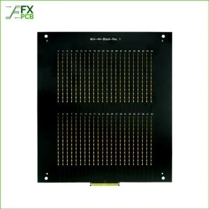
As a fast turnaround or quick-turn PCB Assembly Manufacturer /factory in Shenzhen China, FX PCB is able to fulfill orders in a fast delivery time with our modern technologies used in production.
Our factory carries out the assembly and installation of printed circuit boards to order. During the development and manufacturing process, constant quality control is carried out. We strictly follow your Gerber file and Bom list for your fast turnaround or quick turn PCBA projects, and we will also be glad to suggest you the alternative for your passive components to decrease your cost, but all replacement components need you to approve and make the final decision on whether you want to use them.
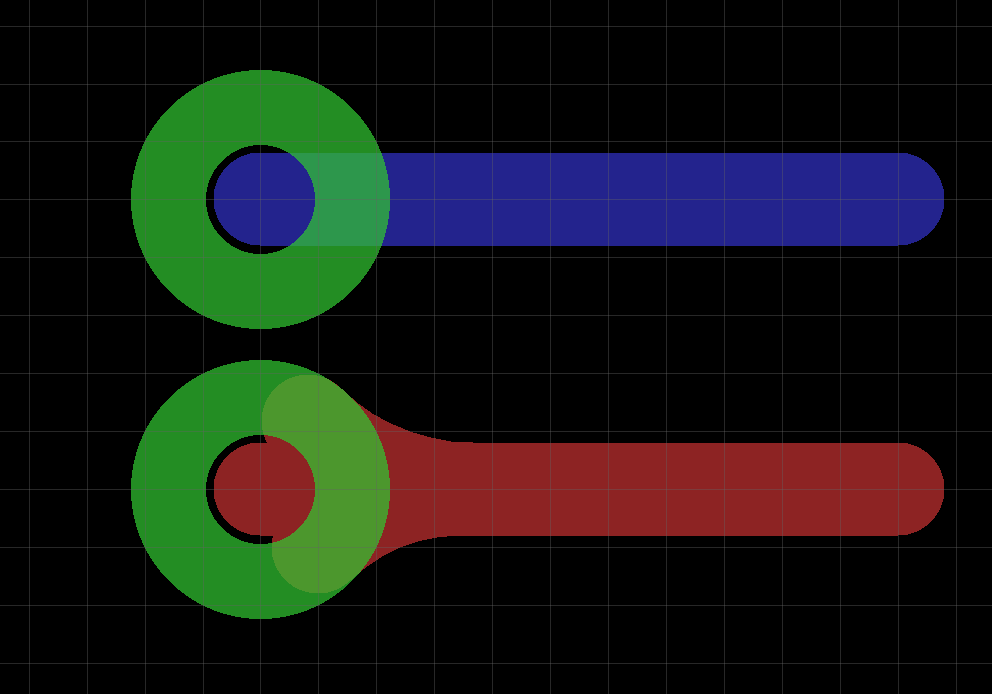
PCB teardrops are not as mysterious as they might sound. Imagine you have a PCB and you want to connect a wire or trace to a hole or via (a hole with conductive material inside). The place where the wire or trace meets the hole might look like a simple connection point. However, PCB designers often modify this connection point to ensure it is robust and dependable.
A PCB teardrop is precisely this modification. Instead of a simple straight-line connection, the copper trace widens gradually as it approaches the hole or via. This widening creates a shape that resembles a teardrop, hence the name.
Now, you might be wondering, why go through the trouble of changing the shape of a connection point on a PCB? Let’s find out.
When copper traces connect to holes or vias, there can be stress concentrations at these points. Think of it like a weak spot in a chain. If too much stress is concentrated in one area, it can lead to cracks or breaks in the copper or the insulating substrate. The teardrop shape helps distribute mechanical stress more evenly, reducing the risk of these problems.
Soldering is the process of joining electrical components to a PCB. For a strong and reliable connection, the solder needs to adhere properly. Teardrop shapes provide more surface area for solder connections. This extra surface area makes it easier for the solder to grip, enhancing the quality and reliability of solder joints.
During the PCB fabrication process, drill bits may slightly deviate from their intended position. This tiny deviation can be a big problem if you have a tight, precise design. Teardrops are like a buffer zone for these deviations. They provide a larger landing area for the drill bit, ensuring that the copper trace still makes a solid connection even if the drill bit doesn’t hit its target spot-on.
In some applications, especially those involving high-frequency signals, maintaining signal integrity is crucial. Teardrop shapes can help with this. They reduce impedance variations at connection points, ensuring that the signal remains strong and consistent as it travels through the PCB.
Ultimately, PCB teardrops contribute to the overall reliability of the PCB. They minimize the chances of open or weak connections, which can lead to electrical issues and, in the worst cases, complete failure of the electronic device.
Now that we understand why PCB teardrops are important, let’s take a look at how they are designed.
PCB designers use specialized software tools to create PCB layouts. These tools often come with features that allow designers to easily implement teardrops where needed. Here’s a simplified breakdown of the design process:
The first step is to identify the connections on the PCB that are critical for the device’s performance. These could be high-current connections, connections carrying sensitive signals, or any other connections where reliability is paramount.
Once the critical connections are identified, the designer uses the PCB design software to apply the teardrop modification. This involves widening the copper traces gradually as they approach the hole or via. The degree of widening depends on the specific design requirements.
While teardrops are valuable for reliability, not all PCB fabrication processes may support them. So, the designer must also consider the manufacturing capabilities and constraints of the chosen PCB fabrication process. It’s a delicate balance between design requirements and manufacturing feasibility.
PCB design is often an iterative process. Designers may go through multiple iterations to optimize the teardrop shapes, ensuring they provide the desired benefits without causing manufacturing issues.
Designing teardrops is one thing, but manufacturing them is another. Let’s explore how PCB teardrops are brought to life during the manufacturing process:
One of the methods used to create teardrops during PCB manufacturing is Laser Direct Imaging (LDI). LDI systems use lasers to expose the photosensitive material on the PCB substrate. This precise process allows for the creation of intricate patterns, including teardrops, with high accuracy.
Depending on the complexity of the design and the desired teardrop shapes, advanced PCB fabrication techniques may be employed. These techniques can include precision etching and plating processes to achieve the desired copper trace shapes.
Throughout the manufacturing process, quality control measures are in place to ensure that the teardrops are correctly formed and meet the design specifications. Any deviations or defects are identified and corrected to maintain the reliability of the PCB.
PCB teardrops find applications in a wide range of electronic devices. Here are a few practical examples to illustrate their importance:
Think of your smartphone or tablet. These devices have densely packed PCBs to accommodate various components. Teardrops help ensure reliable connections between these components and the PCB, reducing the risk of issues like dropped calls or touch screen malfunctions.
Medical devices, such as heart monitors or infusion pumps, require high reliability. Teardrops in their PCBs contribute to the overall safety and effectiveness of these devices.
In aerospace and defense applications, reliability is paramount. Teardrops help maintain the integrity of critical connections in avionics systems, ensuring the safety and performance of aircraft and military equipment.
Modern vehicles rely heavily on electronics for various functions, from engine control to entertainment systems. PCB teardrops help ensure the reliability of these electronics, even in harsh automotive environments.
While PCB teardrops offer several benefits, there are also some common misconceptions associated with them:
Not every connection on a PCB requires a teardrop modification. Designers use them selectively on critical connections where they add value.
Teardrops are valuable but not a guaranteed solution to all PCB reliability issues. They are just one tool in the designer’s toolbox for creating robust PCBs.
Some PCB fabrication processes may not support the creation of teardrops due to their complexity. Designers need to consider the manufacturing capabilities of their chosen fabrication house.
In the world of electronics, reliability is key. PCB teardrops are a small but significant design feature that contributes to the reliability of electronic devices we rely on every day. By distributing mechanical stress, improving soldering, mitigating drill bit deviations, and enhancing signal integrity, teardrops play a crucial role in ensuring that our gadgets and appliances work as expected.

I am Peter Gong. I have been working in PCB and PCBA industry for 15+ years now. I have been a part of the PCB revolution with my dedication to circuit board technologies and creative ideas. I write in FX PCB to impart my knowledge on PCB and PCBA for all circuit board lovers, manufacturers, and users.
WhatsApp us