PCBs (Printed Circuit Boards) are the unsung heroes of modern electronics, silently working behind the scenes to make our gadgets function. However, when a PCB trace—the copper pathways on the board—becomes damaged, it can disrupt the flow of electricity, leading to device malfunctions. In this comprehensive guide, we will take you through the process of PCB trace repair, empowering you to rescue your electronic devices and save on replacement costs.

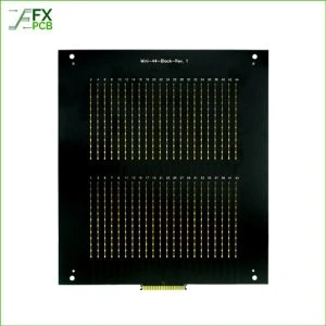
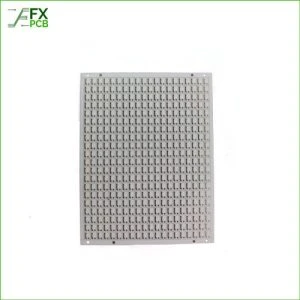
The modern-day electronics world depends heavily on the Printed Circuit Boards (PCBs) as its backbone. A PCB is a medium to transfer the current through its copper pathway and it dissipates the heat to keep the tiny yet highlycomplex electronic equipment on it in perfect condition.
If you are to get the best PCBA and PCB for your digital devices, you have to know this PCB assembly process thoroughly. FX PCB with its years of experience understands this need and thus, we present you the detailed guideline.
FX PCB dont follow the standerd manufacturing process is no exception to it. Our process includes solder pasting on the PCB base, placing the electronic components in the right place, soldering them with the PCB, checking the accuracy, final inspection, and delivery to customers.
Before we jump into the repair process, it’s crucial to grasp the fundamentals.
PCB traces are thin copper lines etched onto the surface of a PCB. These lines act as the conductive pathways that allow electrical current to flow between various components on the board. In essence, they are the roads that electricity travels on within your electronic devices.
PCB traces are vital because they enable the proper functioning of electronic circuits. When a PCB trace gets damaged, it can interrupt the flow of electrical signals, causing malfunctions or rendering the device non-operational. Common causes of PCB trace damage include physical stress, corrosion, aging, and soldering errors.
To repair PCB traces effectively, you’ll need the right tools and materials. Here’s what you’ll require:
This diagnostic tool helps you identify damaged traces and verify their repair by measuring continuity.
Choose a quality soldering iron with adjustable temperature settings for precise soldering.
Use fine-gauge soldering wire with flux to ensure clean and reliable solder joints.
These tools, like a desoldering braid and a desoldering pump, are essential for removing excess solder when necessary.
These aids help you inspect small, intricate traces in detail.
Use this for cleaning the PCB before and after repair to maintain a pristine work surface.
Keep spare copper traces or fine copper wire on hand for situations where direct repair is impossible.
This insulation solution protects repaired areas from shorts and further damage.
Apply this protective layer to safeguard against moisture, dust, and environmental factors.
Use anti-static wrist straps and mats to prevent electrostatic discharge that can harm sensitive components.

Now, let’s dive into the step-by-step process of repairing damaged PCB traces:
Visual Inspection
Begin by carefully examining the PCB for visible signs of damaged traces, such as cracks, breaks, or corrosion. If necessary, use a magnifying glass or microscope to spot tiny imperfections that might be missed with the naked eye.
Locate the Damage
To pinpoint the exact location of the damaged trace, use a multimeter in continuity mode. This mode emits a beep when it detects a continuous path, helping you find the break in the trace.
Clean the Area
Before soldering, clean the damaged area and its surroundings with isopropyl alcohol to ensure a clean and contaminant-free work surface.
Soldering
Bypassing the Trace
Insulation
Testing
Here are some best practices to ensure a successful PCB trace repair:
Precision and Patience: PCB repair demands a steady hand and patience. Take your time to avoid mistakes.
Practice: If you’re new to PCB repair, practice on scrap PCBs or non-critical devices to hone your skills.
Safety First: Work in a well-ventilated area, wear safety goggles, and exercise caution when handling a hot soldering iron.
Documentation: Keep detailed notes and diagrams of the repair process, especially for complex PCBs with multiple traces.
Temperature Control: Avoid overheating the PCB by using the lowest effective soldering temperature.
Double-Check: After repairing the trace, thoroughly inspect your work to eliminate solder bridges or unintended connections.
Repairing PCB traces is a valuable skill for electronics enthusiasts and professionals. With the right tools, materials, and techniques, you can diagnose and mend damaged traces effectively, extending the lifespan of your electronic devices and saving on replacement costs. PCB trace repair is a combination of precision, patience, and practice, and as you become more experienced, you’ll find it to be a rewarding and cost-effective solution for keeping your electronics in working order.
Related: PCBA, Ceramic PCB, Glass PCB

I am Peter Gong. I have been working in PCB and PCBA industry for 15+ years now. I have been a part of the PCB revolution with my dedication to circuit board technologies and creative ideas. I write in FX PCB to impart my knowledge on PCB and PCBA for all circuit board lovers, manufacturers, and users.
WhatsApp us