Printed Circuit Boards (PCBs) are the backbone of modern electronics, serving as the foundation for connecting and supporting electronic components. Among various types of PCBs, the Cavity PCB, also known as embedded PCB or cavity boards, has gained significant prominence. This article explores what cavity PCBs are, their different types, advantages, applications, and the manufacturing process behind them.

As a fast turnaround or quick-turn PCB Assembly Manufacturer /factory in Shenzhen China, FX PCB is able to fulfill orders in a fast delivery time with our modern technologies used in production.
Our factory carries out the assembly and installation of printed circuit boards to order. During the development and manufacturing process, constant quality control is carried out. We strictly follow your Gerber file and Bom list for your fast turnaround or quick turn PCBA projects, and we will also be glad to suggest you the alternative for your passive components to decrease your cost, but all replacement components need you to approve and make the final decision on whether you want to use them.
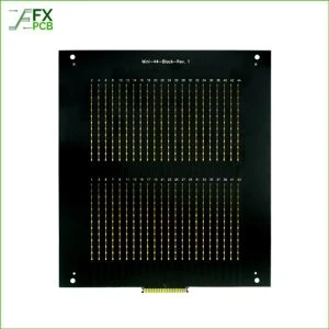
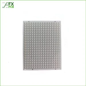
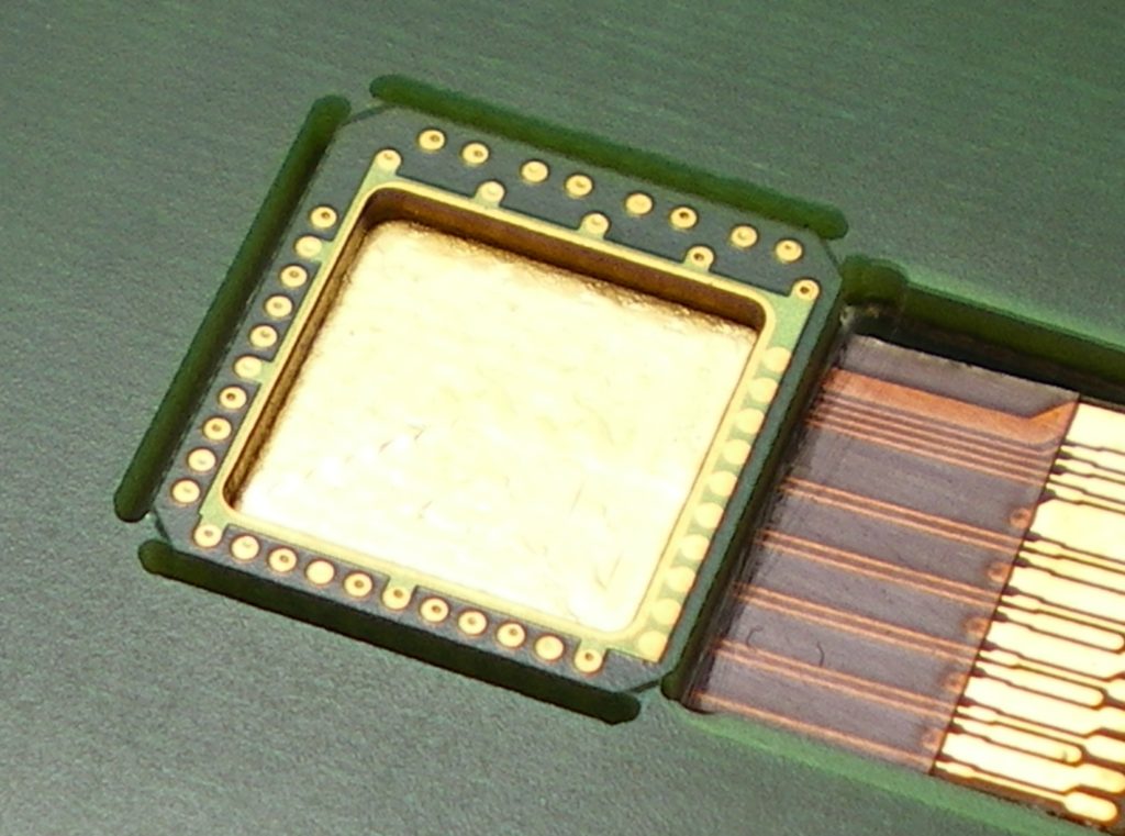
A Cavity PCB, short for Cavity Printed Circuit Board, is a specialized type of PCB that features one or more cavities or recesses within the board itself. These cavities are created by removing specific sections of the PCB substrate material, which can be made of materials like FR-4, Rogers, or other substrates. These cavities are designed to house electronic components, which are then encapsulated to protect them and reduce the overall profile of the PCB.
Cavity PCBs can be categorized into several types, depending on their specific design and application:
Blind cavity PCBs have cavities that do not penetrate through the entire PCB. These are ideal for applications where components need to be partially embedded while maintaining a flat surface on the opposite side of the board.
Blind cavity PCBs are frequently used in mobile devices where various components, like the camera module or sensors, need to be partially recessed into the PCB to achieve a sleek, flat design. The recessed components allow for a smoother, more streamlined exterior design.
Buried cavity PCBs have cavities that are entirely enclosed within the board and do not extend to the outer layers. This design is often used to reduce the overall thickness of the PCB and protect sensitive components.
In high-density electronics, such as high-performance laptops or medical devices, designers use buried cavity PCBs to create a thinner profile without compromising the integrity of the components. By encapsulating components within the PCB layers, these boards can be made thinner, improving the overall form factor.
Through cavity PCBs have cavities that extend from one side of the board to the other, providing easy access for component placement and removal. These are commonly used in applications where components need to be mounted on both sides of the PCB.
In telecommunications equipment, for example, where space is limited, through cavity PCBs offer a solution to house components on both sides of the board. The through-cavity design enables efficient use of board space and allows for greater component density.
Cavity PCBs offer several advantages that make them desirable for various applications:
The primary advantage of cavity PCBs is their ability to reduce the overall height of a device by embedding components within the PCB. This is particularly useful in applications with strict space constraints.
In the automotive industry, for instance, where designers aim to make sleek, low-profile infotainment systems, cavity PCBs are instrumental. By embedding components like touchscreen controllers and interface connectors within the PCB, automotive displays can maintain a slim, aesthetically pleasing design.
Cavity PCBs can help in dissipating heat generated by embedded components more effectively, as the PCB itself acts as a heat sink.
In the field of power electronics, thermal management is crucial to maintaining component reliability. Cavity PCBs are employed to create compact, efficient power modules. The design allows components to be mounted close to the PCB’s metal core, enhancing heat dissipation and ensuring long-term performance.
Components housed within cavities are shielded from external factors, improving their reliability and protection against environmental elements.
In the aerospace and defense sector, where electronics must perform reliably in extreme conditions, cavity PCBs are used to safeguard critical components. These boards are often sealed with ruggedized enclosures, ensuring that sensitive electronics are shielded from moisture, dust, and other environmental threats.
The reduced electromagnetic interference and shorter signal paths within cavity PCBs can enhance the signal integrity and reduce cross-talk.
Data centers rely on cavity PCBs to maintain the highest levels of signal integrity in their servers and networking equipment. By carefully designing cavity layouts and reducing electromagnetic interference, these PCBs ensure reliable data transmission and minimal data loss.
Cavity PCBs allow for efficient use of board space, enabling designers to pack more functionality into smaller devices.
In the field of IoT (Internet of Things) devices, where compact design is a priority, cavity PCBs are used to maximize space utilization. This allows designers to include various sensors, wireless modules, and microcontrollers in a small footprint, making IoT devices more versatile and cost-effective.
Cavity PCBs find applications in various industries and sectors, including:
Manufacturing cavity PCBs involves specialized processes, including:
Cavity PCBs represent a significant advancement in PCB technology, allowing for more compact and reliable electronic devices across a range of industries. Their unique advantages, diverse applications, and specialized manufacturing processes make them a valuable choice for engineers and designers working on cutting-edge electronic products. As technology continues to evolve, we can expect cavity PCBs to play an even more prominent role in the design of smaller, more efficient, and more powerful electronic devices. Whether in aerospace, healthcare, telecommunications, or consumer electronics, cavity PCBs are making their mark in shaping the future of technology.

I am Peter Gong. I have been working in PCB and PCBA industry for 15+ years now. I have been a part of the PCB revolution with my dedication to circuit board technologies and creative ideas. I write in FX PCB to impart my knowledge on PCB and PCBA for all circuit board lovers, manufacturers, and users.
WhatsApp us