In the rapidly advancing landscape of electronics, innovation is the driving force behind smaller, more powerful, and energy-efficient devices. Among the many technological breakthroughs that have propelled this evolution, Ball Grid Array (BGA) printed circuit boards (PCBs) stand out as a pivotal development. These compact and high-performance PCBs have revolutionized the design and manufacturing of electronic devices. In this article, we will explore the history, working principles, advantages, considerations, and future prospects of BGA PCBs.

The modern-day electronics world depends heavily on the Printed Circuit Boards (PCBs) as its backbone. A PCB is a medium to transfer the current through its copper pathway and it dissipates the heat to keep the tiny yet highlycomplex electronic equipment on it in perfect condition.
If you are to get the best PCBA and PCB for your digital devices, you have to know this PCB assembly process thoroughly. FX PCB with its years of experience understands this need and thus, we present you the detailed guideline.
FX PCB dont follow the standerd manufacturing process is no exception to it. Our process includes solder pasting on the PCB base, placing the electronic components in the right place, soldering them with the PCB, checking the accuracy, final inspection, and delivery to customers.
The concept of BGA technology dates back to the early 1960s when IBM first introduced it for their large-scale mainframe computers. However, it wasn’t until the late 1980s and early 1990s that BGA packaging gained significant traction in the consumer electronics market. This growth was driven by the need for smaller form factors in products like laptops, mobile phones, and game consoles.
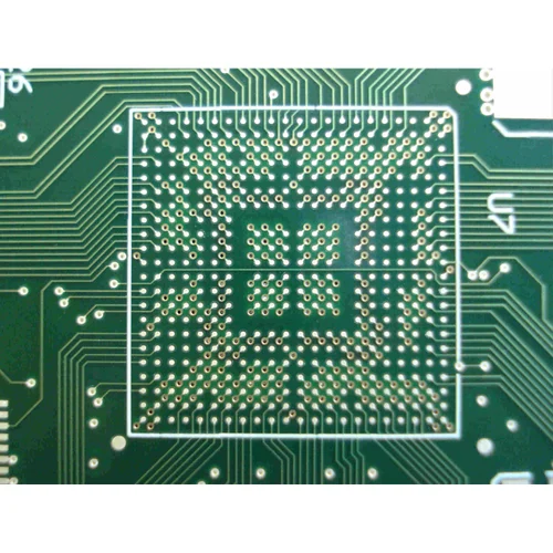
At its core, a Ball Grid Array PCB is a type of integrated circuit (IC) packaging and interconnection technology used in printed circuit boards. What sets BGA apart is the arrangement of numerous small solder balls on the bottom side of the IC package. These solder balls are precisely positioned in a grid pattern, giving rise to the name “Ball Grid Array.”
The functionality of a BGA PCB is deceptively simple. The IC is attached to the PCB by aligning the solder balls on the IC package with matching pads on the PCB. This precise alignment ensures that each solder ball establishes a secure and low-resistance connection between the IC and the PCB. The assembly then undergoes a controlled reflow soldering process, during which the solder balls melt and solidify, firmly anchoring the IC in place.
The widespread adoption of BGA PCBs can be attributed to their numerous advantages:
BGA technology’s most celebrated feature is its ability to achieve a high-density interconnect. By employing a closely spaced array of solder balls, BGAs reduce the overall footprint of the PCB. This compactness is invaluable in modern electronics, where size constraints are paramount.
Shorter trace lengths in BGA designs translate into reduced signal propagation delays and attenuations. This results in improved signal integrity and reduced susceptibility to electromagnetic interference (EMI). BGAs are particularly well-suited for high-frequency and high-speed applications.
The multitude of solder balls in a BGA package serves as efficient pathways for heat transfer. This design feature facilitates the effective dissipation of heat generated by the IC, a critical factor in power-hungry components in contemporary electronic devices.
BGA components exhibit remarkable resilience against mechanical stresses and vibrations. This durability surpasses that of alternative interconnection methods like through-hole technology, making BGAs a favored choice for applications exposed to harsh operating conditions.
BGA packages can accommodate a larger number of pins or connections. This makes them indispensable for complex ICs such as microprocessors, FPGAs, and other system-on-chip (SoC) devices.
While the advantages of BGA PCBs are clear, their integration requires careful consideration of certain factors:
Soldering Complexity: The soldering of BGAs necessitates precise techniques and specialized equipment. This includes reflow soldering ovens with meticulously controlled temperature profiles. Inadequate soldering practices can lead to defects like solder bridging or cold joints, jeopardizing the reliability of the PCB.
Inspection and Testing Challenges: The concealed nature of solder joints beneath the IC package complicates inspection and testing. X-ray inspection is often employed to ensure the quality of solder joints, adding an extra layer of complexity to the manufacturing process.
Repair Difficulty: Unlike through-hole components that are relatively easy to replace or repair, BGAs present a greater challenge in this regard. The intricate soldering involved can make rework complex, potentially increasing maintenance costs and reducing the overall repairability of electronic devices.
Thermal Management: While BGAs enhance heat dissipation, it is essential to implement appropriate thermal management solutions. These may include heat sinks, thermal vias within the PCB, or advanced cooling systems to prevent overheating of critical components.
Signal Integrity Design: Achieving optimal signal integrity in BGA-based designs necessitates meticulous planning. This includes selecting suitable PCB materials, designing controlled impedance traces, and managing signal routing to minimize crosstalk and signal loss.
Cost Considerations: BGAs can be more expensive to manufacture and repair due to the specialized equipment and expertise required. Designers must carefully weigh these costs against the benefits of using BGA technology for their specific application.
As technology continues to evolve, BGA PCBs are poised to play an increasingly vital role in electronic design. Several emerging trends and future developments point to the continued growth of this technology:
Miniaturization: In response to consumer demand for smaller, more portable devices, BGA technology will continue to be instrumental in achieving miniaturization goals. This trend is especially evident in the development of wearables, Internet of Things IoT devices, and mobile electronics.
High-Performance Computing: BGA packages will remain the go-to choice for high-performance computing applications. Their ability to handle high pin counts and efficiently dissipate heat makes them indispensable for cutting-edge processors and memory modules.
5G and Beyond: The rollout of 5G networks and the increasing demand for high-speed data transmission will further drive the adoption of BGA technology. BGAs will find use in advanced RF components and high-frequency modules.
Automotive Electronics: The automotive industry will increasingly leverage BGA PCBs due to their reliability and ability to withstand harsh environmental conditions. These boards will be incorporated into advanced driver-assistance systems (ADAS), infotainment systems, and electric vehicle components.
Medical Devices: Miniaturized, high-performance medical devices will benefit from BGA technology. These devices will provide improved diagnostic capabilities and treatment options.
In conclusion, Ball Grid Array (BGA) PCBs have become a linchpin in the modern electronics landscape, offering a myriad of advantages that address the demands of today’s electronics industry. Nevertheless, their adoption necessitates a nuanced understanding of soldering techniques, inspection and testing protocols, repair intricacies, and thermal management. As technology continues its relentless march forward, BGA technology is poised to play a pivotal role in enabling smaller, more potent, and more energy-efficient electronic devices across diverse industries.
Related: PCBA, Glass PCB, Ceramic PCB

I am Peter Gong. I have been working in PCB and PCBA industry for 15+ years now. I have been a part of the PCB revolution with my dedication to circuit board technologies and creative ideas. I write in FX PCB to impart my knowledge on PCB and PCBA for all circuit board lovers, manufacturers, and users.
WhatsApp us