Introduction
Moving to a 12-layer PCB is not a routine upgrade. Engineers make this call when lower-count boards have failed to solve real electrical problems — BGA breakout congestion, EMI compliance failures, or signal integrity degradation on high-speed interfaces that cleaner routing alone cannot fix.
A 12-layer board consists of 12 alternating copper and dielectric layers laminated into a single board. It's one of the more demanding multilayer configurations in standard PCB manufacturing, and the decisions made before fabrication begins — stack-up arrangement, material selection, via strategy — directly determine whether the finished board performs as designed or requires costly respins.
What follows covers the full design and manufacturing picture: stack-up logic, fabrication sequence, material tradeoffs, and the quality factors that most affect yield at this layer count.
Key Takeaways
- A 12-layer PCB uses 12 alternating copper and dielectric layers, optimized for high-density routing, signal integrity, and power distribution
- Engineers move to 12 layers when 8–10 layer boards can't handle BGA routing complexity, EMI control, or high-speed interface demands
- Stack-up design (layer sequence, reference planes, dielectric selection) is the most consequential decision before fabrication
- Fabrication spans inner layer imaging, lamination cycles, drilling, via plating, outer layer processing, and full electrical testing
- Material choice, via structure, copper symmetry, and DFM validation are the four variables that most affect final board reliability
What Is a 12-Layer PCB and When Do You Need One?
A 12-layer PCB is a printed circuit board built from 12 alternating copper and dielectric layers (prepreg and core), compressed under heat and pressure into one rigid panel. Each copper layer carries a defined function: signal routing, power distribution, or ground reference.
Why Not Stay at 8 or 10 Layers?
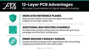
The extra layers provide three things that lower-count boards cannot:
- Dedicated reference planes adjacent to every high-speed signal layer, keeping ground and power clean
- Additional routing channels for high-density BGA escape routing where via-to-via spacing is already tight
- Inner ground planes that act as Faraday shields between signal layers, improving EMI containment
Xilinx's UG583 PCB design guide notes that PCBs for large FPGAs typically range from 12 to 22 layers, with total layer count determined by signal layer requirements plus power and ground planes. 12 layers is typically the starting point for complex FPGA-class designs, not the ceiling.
Engineering Triggers That Justify 12 Layers
You're likely ready for 12 layers when you encounter:
- High pin-count BGA breakout that 8-layer routing cannot resolve without violating impedance rules
- DDR or PCIe routing that requires uninterrupted reference plane continuity across the board
- Signal integrity failures during prototype testing on a 10-layer design
- EMI compliance failures that split ground planes at lower layer counts cannot fix
- Layer count guidance from your FPGA or processor vendor's reference design
Layer count should be determined by routing density and electrical requirements. Adding layers without a clear stack-up rationale increases fabrication cost and can introduce manufacturing complexity with no measurable performance return. The next step is defining a stack-up that puts those 12 layers to work.
12-Layer PCB Stack-up: Layer Arrangement and Design Strategy
A PCB stack-up is the predefined sequence of copper layers and dielectric materials that forms the board before routing begins. It is both an electrical decision and a manufacturing constraint. Once fabrication starts, it cannot be changed.
A Common 12-Layer Stack-up Pattern
A widely used arrangement places high-speed signal layers adjacent to solid reference planes:
| Layer | Function |
|---|---|
| L1 | Signal (outer) |
| L2 | Ground |
| L3 | High-speed signal |
| L4 | Signal |
| L5 | Power |
| L6 | Ground |
| L7 | Ground |
| L8 | Power |
| L9 | Signal |
| L10 | High-speed signal |
| L11 | Ground |
| L12 | Signal (outer) |
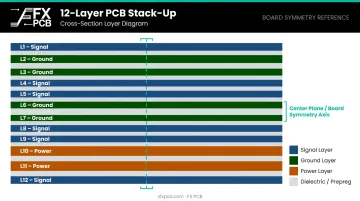
High-speed layers (L3, L10) sit between solid ground planes to minimize return path length and control crosstalk. Power and ground layers cluster toward the center for clean distribution. This arrangement is illustrative — your actual stack-up must be validated against your specific routing, impedance, and material constraints.
Symmetry and Warpage
Stack-up symmetry is not optional. Symmetric copper weight and dielectric thickness around the board's center plane reduce differential thermal expansion during lamination and reflow. Asymmetric designs warp, and warpage on a 12-layer board is difficult to correct after lamination. IPC-TM-650 2.4.22C defines standard measurement procedures for bow and twist in rigid printed boards.
Impedance Control Through the Stack-up
Characteristic impedance is set by three variables:
- Trace width on the signal layer
- Dielectric constant (Dk) of the prepreg or core between the trace and its reference plane
- Distance between the trace and the reference plane
Impedance targets are interface-specific — not universal. Xilinx UG583 lists DDR4 breakout routing at 50 ohm ±10%, analog differential pairs at 100 ohm ±7%, while TI's PCIe Gen 5 layout guide targets 85 ohm differential. Stack-up impedance calculations using field solvers are estimates — actual fabricated impedance depends on laminate Dk tolerances and resin flow during lamination. Confirm targets with your manufacturer before final stack-up approval.
Via Strategy
Via type directly affects routing density and fabrication cost:
- Through-hole vias — connect all 12 layers, simplest and lowest cost to manufacture
- Blind vias — connect an outer layer to one or more inner layers, invisible from the opposite side
- Buried vias — connect inner layers only, not visible on either outer surface
Blind and buried vias are necessary for high-density BGA layouts where through-hole vias consume too much routing space. They require sequential lamination cycles, which adds cost and lead time. According to Intel's board design guidelines, blind vias can reduce required layer counts because signals can route beneath them — which means via strategy and layer count decisions are interdependent.
The 12-Layer PCB Fabrication Process
Fabrication follows a fixed sequence where each stage depends on the one before it. Errors at lamination are permanent — once the panel is bonded, there is no correcting internal layer defects.
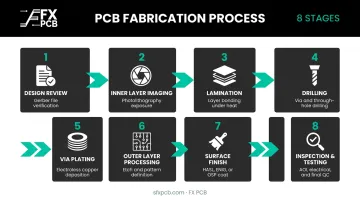
The full process runs in this order:
- Design review and Gerber file preparation
- Inner layer imaging and etching
- Lamination (sequential cycles for blind/buried via designs)
- Mechanical and laser drilling
- Via plating (electroless copper + electroplating)
- Outer layer processing
- Surface finish application
- Inspection and electrical testing
Inner Layer Processing
Inner layers are imaged using photolithography: a circuit pattern is exposed onto copper-clad laminate, then chemically etched to remove unwanted copper and reveal the desired traces and planes. AOI is performed on every inner layer before bonding to catch opens, shorts, and linewidth deviations while corrections are still possible.
Lamination
Inner layer cores and prepreg sheets are stacked in sequence on alignment pins, then pressed under controlled heat and pressure to cure the resin and bond all layers into a single panel. Process parameters are material-specific: Panasonic MEGTRON 6, for example, requires product temperature above 185°C for at least 75 minutes, with pressure ranging from 3.0 to 4.0 MPa depending on heat-up rate. Isola 370HR targets a lower peak temperature range, typically 170–180°C, under its own press profile.
For 12-layer boards with blind or buried vias, lamination occurs in sequential cycles: sub-composites are built and drilled first, then outer layers are added in subsequent press cycles.
Drilling and Via Plating
Mechanical drilling handles standard through-hole vias; laser drilling creates microvias for HDI structures. SFX PCB supports a maximum aspect ratio of 16:1, with mechanical drilling down to 0.15 mm and laser drilling to 0.1 mm (4 mil) for low-volume production.
Via plating runs in two stages: electroless copper deposits a conductive seed layer inside drilled holes, then electroplating builds copper to specification. Cross-section analysis verifies copper thickness on via walls. High aspect ratios present plating challenges. Intel's BGA routing guidelines list 10:1 as a premium aspect ratio threshold for flip-chip BGA designs, beyond which plating reliability requires process verification.
Outer Layer Processing, Surface Finish, and Testing
Outer layers undergo the same photolithography and etching process as inner layers, followed by solder mask application and silkscreen. Surface finish options available from SFX PCB include:
- HASL — cost-effective, good solderability, less flat surface
- ENIG — flat, excellent for fine-pitch components, longer shelf life (governed by IPC-4552)
- OSP — RoHS-compliant, flat, shorter shelf life (governed by IPC-4555)
- Immersion Silver / Immersion Tin / ENEPIG — application-specific
Testing closes out fabrication: 100% electrical continuity testing is performed on every bare board at SFX PCB before shipping, detecting open circuits and shorts. AOI covers outer layer defects; X-ray inspection verifies buried via integrity and is particularly valuable for BGA-area via structures that cannot be visually inspected.
Key Design and Manufacturing Factors That Affect Quality
Material Selection
| Material | Tg | Dk (at 1 GHz) | Df (at 2 GHz) | Best For |
|---|---|---|---|---|
| Standard FR-4 (Isola FR406) | ~135°C | ~4.2 | Higher | Consumer / industrial <1 GHz |
| High-Tg FR-4 (Isola 370HR) | 180°C | 4.17 | 0.0210 | High-layer-count industrial |
| Panasonic MEGTRON 6 | 185°C (DSC) | 3.71 | Low-loss | High-speed, 5G, server boards |
| Rogers RO4003C | Thermoset | ~3.38 | ~0.0027 at 10 GHz | RF, microwave |
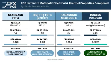
SFX PCB sources from multiple laminate suppliers including Isola, Rogers, Panasonic, ITEQ, and Shengyi — material selection for your stack-up can be confirmed during the quoting process.
Controlled Impedance Verification
Stack-up calculations are starting points, not guarantees. Actual fabricated impedance shifts based on laminate Dk lot-to-lot variation and resin flow during lamination. Best practice: include impedance test coupons on the panel edge and require TDR coupon testing before boards are released for assembly.
SFX PCB performs impedance control testing using TDR equipment to ±10% tolerance, with results documented for each production lot.
DFM as a Quality Gate
DFM issues that commonly reduce 12-layer yield:
- Uneven copper distribution between adjacent layers causing warpage
- Excessive via density under BGA pads with no copper fill process specified
- Stacked vias without confirming the manufacturer's fill capability
- Annular ring violations at minimum drill sizes
- High-speed traces crossing split planes — Intel AN 958 explicitly prohibits this, noting it extends return paths and increases trace inductance
A DFM review before Gerber release — not after — is the single most effective action to prevent respins.
SFX PCB provides free DFM analysis on every order. ISO9001, ISO13485, and IPC-A-610 Class 2/3 certifications back the process controls that make that review meaningful.
Common Fabrication Challenges and Misconceptions
Adding layers isn't a performance shortcut. 12-layer boards add cost, complexity, and lead time — they're justified only when specific routing, power distribution, or EMI problems require it. Before committing to 12 layers, verify that a simpler stack-up can't solve the same problems at lower cost.
The Three Most Common 12-Layer Manufacturing Failures
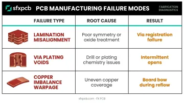
Lamination misalignment: Poor stack-up symmetry or inconsistent oxide treatment of inner layers shifts layer registration. The result — vias that miss their targets — only shows up electrically, making these failures expensive to diagnose.
Via plating voids: When drill parameters or plating bath chemistry aren't calibrated for board thickness, deep holes develop internal voids. These create intermittent opens that resist standard electrical testing and typically require destructive cross-section analysis (physically slicing the board) to confirm.
Copper weight imbalance causing warpage: Uneven copper coverage between adjacent layers produces different thermal expansion rates during reflow. A dense signal layer paired with a sparse power plane creates mechanical stress — the board bows as it heats and cools.
Most of these failures trace back to decisions made before the board reaches the factory floor.
Design-Stage Mistakes That Create Manufacturing Problems
- Routing high-speed traces across split planes (creates return path discontinuity and EMI radiation)
- Specifying stacked vias without confirming the manufacturer's copper fill process capability
- Minimum annular rings or drill sizes that exceed the fabricator's verified tolerance
- Failing to validate impedance targets against actual material lots before mass production
Frequently Asked Questions
What is the standard board thickness for a 12-layer PCB?
Finished thickness for 12-layer boards commonly falls between 1.6 mm and 2.4 mm, with 1.6 mm typical for standard designs and thicker boards used when copper weight or controlled impedance requires additional dielectric spacing. Final thickness must be agreed with your manufacturer before fabrication begins.
How much does a 12-layer PCB cost compared to an 8-layer board?
12-layer boards cost considerably more due to additional lamination cycles, greater material volume, tighter registration tolerances, and lower per-panel yield. Exact pricing depends on quantity, material grade, via complexity, and surface finish. Contact SFX PCB directly for a manufacturer quote with transparent pricing.
What materials are used in a 12-layer PCB stack-up?
Standard 12-layer boards use FR-4 cores and prepreg with copper foil. High-speed or high-temperature applications require upgraded materials: High-Tg FR-4 (such as Isola 370HR at Tg 180°C), low-loss laminates (Panasonic MEGTRON 6), or hybrid stack-ups that place premium materials only on critical signal layers.
What is the typical lead time for 12-layer PCB fabrication?
Standard production lead times generally range from 7 to 15 working days, with expedited prototype options available in as few as 5 days depending on complexity and capacity. Designs with blind/buried vias or special laminates require additional time due to sequential lamination cycles.
When should I use blind and buried vias in a 12-layer PCB?
Use blind and buried vias when through-hole vias consume too much routing space — typically with high-density BGAs, tight-pitch components, or constrained board real estate. They increase cost and require sequential lamination, so specify them only when through-hole routing clearly cannot meet density requirements.
Can standard FR-4 be used for all 12-layer PCB applications?
Standard FR-4 (Tg ~135°C) works well for most industrial applications with moderate thermal cycling. For high-speed designs (PCIe Gen 4+, DDR5, 5G) or IPC-6012 Class 3 applications in aerospace or medical, specify High-Tg or low-loss laminates. This prevents signal degradation and delamination under thermal stress.