Introduction
Multilayer PCB manufacturing transforms digital design files into a physically tested circuit board with three or more conductive copper layers. Unlike single or double-sided boards, multilayer fabrication laminates copper and dielectric layers into a single rigid structure, where every stage depends on the one before it.
This guide is written for engineers, product designers, and procurement teams working in automotive, medical devices, consumer electronics, and industrial automation — sectors where board complexity, signal integrity, and reliability aren't optional.
What follows covers every major fabrication stage in sequence — what happens, why it matters, and where production errors most often originate.
Key Takeaways
- Multilayer PCBs (4, 6, 8+ layers) enable compact, high-performance designs by stacking copper layers separated by prepreg and laminate core.
- Manufacturing follows a fixed sequence — from DFM review and inner layer imaging through lamination, drilling, plating, surface finish, and final electrical testing.
- Each stage is interdependent — a lamination misalignment directly compromises via registration and electrical continuity.
- Cost and quality are driven by layer count, via types, copper weight, material selection, and lamination cycle count.
- Free DFM analysis before production and 100% electrical testing on every bare board are the two highest-impact quality checkpoints.
What Is a Multilayer PCB?
A multilayer PCB is any printed circuit board with three or more conductive copper layers, alternating with insulating dielectric layers (prepreg and laminate core), bonded into a single rigid structure under heat and pressure, governed by IPC-6012F, the current qualification and performance specification for rigid printed boards.
How It Differs From Single and Double-Sided Boards
Single and double-layer boards route all signals on one or two surfaces. Multilayer boards route signals across multiple planes, enabling:
- Dedicated ground and power planes that suppress EMI and stabilize power delivery
- Higher component density through reduced board footprint
- Shorter signal paths that improve high-speed performance
Most commercial multilayer boards run 4 to 14 layers. Advanced applications (servers, aerospace avionics, high-frequency RF systems) can exceed 20 to 30 layers. OKI recently demonstrated 124-layer PCB technology targeting next-generation AI and high-speed processing — a benchmark that signals where density requirements are heading.
Each additional layer adds measurable manufacturing complexity, cost, and registration tolerance demands.
That complexity hasn't slowed adoption. The global multilayer PCB market was valued at $71 billion in 2023, projected to reach $116.1 billion by 2032 at a 5.5% CAGR, driven by 5G infrastructure, ADAS automotive systems, and medical imaging electronics — all applications that depend on the signal integrity and density multilayer construction provides.
The Multilayer PCB Manufacturing Process: Step by Step
Step 1: DFM Analysis and CAM Processing
Manufacturing begins before a single panel is touched.
Customers submit design files — Gerber is the standard open format for PCB design data transfer, per Ucamco's official specification; ODB++ and IPC-2581 formats are also accepted by advanced manufacturers. SFX PCB accepts Gerber, Eagle, and CAD files across its multilayer product lines.
The manufacturer's engineering team runs a DFM (Design for Manufacturability) check to identify issues including:
- Trace widths below process minimums
- Insufficient annular rings or pad sizing errors
- Via placements that conflict with pads
- Stack-up imbalances that cause warpage
- Copper distribution problems across layers
Errors caught here take minutes to fix. The same errors found after lamination result in scrapped panels.
CAM processing follows DFM sign-off. It converts corrected design data into production-ready imaging files, generates drill programs, verifies stack-up, confirms impedance targets, and creates the manufacturing traveler (the document that follows the panel through every production station).
SFX PCB provides free DFM analysis with every order, enabling engineers to resolve design issues before a single panel is processed.
Step 2: Material Selection and Stack-Up Definition
The stack-up defines the layer arrangement of copper foil, prepreg sheets (uncured resin-impregnated glass fabric), and laminate cores (cured copper-clad substrate). This determines final board thickness, dielectric properties, and impedance characteristics.
Material selection by application:
| Material | Use Case | Key Properties |
|---|---|---|
| FR-4 (e.g., Isola IS410) | Standard commercial | Tg 180°C, Dk 3.97, Df 0.020 at 2 GHz |
| Rogers RO4003C | RF / high-frequency | Dk 3.38 ±0.05, Df 0.0027 at 10 GHz |
| Rogers RT/duroid 5880 | Millimeter-wave, low loss | Dk 2.20 ±0.02, Df 0.0009 at 10 GHz |
| High-Tg laminates | Thermal-demanding designs | Tg 150–180°C options |
SFX PCB regularly processes FR-4, Rogers RO4003C, RO4350B, PTFE-based laminates, and high-Tg variants (Tg150, Tg170, Tg180) from suppliers including Isola, Rogers, ITEQ, Ventec, and Arlon.
Stack-up decisions made at this stage affect every downstream step. Unbalanced copper distribution causes warpage during lamination. Incorrect prepreg selection produces impedance deviations. Core thickness choices constrain via aspect ratios and drilling tolerances.
Step 3: Inner Layer Imaging, Etching, and AOI
Each inner layer core goes through the same sequence:
- Clean — copper-clad laminate is chemically cleaned to remove oxides and contaminants
- Coat — photosensitive resist film is applied to both sides
- Expose — Laser Direct Imaging (LDI) selectively hardens the resist according to the CAD circuit pattern; SFX PCB achieves inner layer trace widths and spacing down to 2.5 mil / 2.5 mil for low-volume production
- Develop — unhardened resist is washed away, exposing the copper to be removed
- Etch — exposed copper is chemically etched, leaving only the desired traces
- Strip — remaining resist is removed to reveal the patterned copper layer
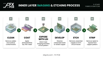
Every inner layer core then undergoes Automated Optical Inspection (AOI). High-definition cameras scan each layer and compare against CAD data, catching shorts, opens, and trace defects before lamination.
This is the last opportunity to correct inner layer defects. Once the board is laminated, those layers are inaccessible.
Step 4: Layer Lamination
Lamination bonds all layers into a single, unified panel. The sequence:
- Inner layer cores receive oxide surface treatment to promote adhesion
- Cores are stacked alternately with prepreg sheets and copper foil in precise sequence using alignment pins
- The completed "book" loads into a hydraulic press under controlled heat and pressure (Isola's IS410 processing guidance specifies a 190°C cure temperature maintained for at least 45 minutes, at 200–400 psi)
- The cured prepreg resin bonds all layers into one rigid structure
Why this step is a quality-critical bottleneck:
- Layer misregistration during stacking compromises via alignment throughout the board
- Inconsistent press parameters (temperature ramp, dwell time, pressure profile) cause resin voids or delamination
- Each additional lamination cycle for blind/buried via builds adds roughly one week to lead time per cycle, per PCB007's reporting on sequential lamination in HDI manufacturing
Step 5: Drilling and Via Formation
CNC machines drill holes using programs that specify each hole's X-Y coordinate, diameter, and depth.
Via types and their manufacturing implications:
- Through-hole vias — drilled top to bottom in a single pass; lowest cost
- Blind vias — connect an outer layer to one or more inner layers; require laser drilling for smaller diameters (SFX PCB achieves 4 mil / 0.10 mm laser-drilled minimum)
- Buried vias — connect inner layers only, invisible from the board surface; require sequential lamination cycles before and after drilling
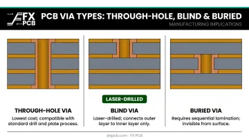
SFX PCB supports blind and buried vias on 6-layer, 8-layer, and higher-count boards, with mechanical drilling down to 0.15 mm and maximum aspect ratio of 16:1.
The desmear process follows drilling. Mechanical drilling generates heat that melts and smears resin onto hole walls; a chemical clean removes that residue before copper deposition, protecting inter-layer connectivity.
Step 6: Copper Plating and Outer Layer Processing
Metallization sequence:
- Electroless copper deposition — a chemical process deposits a thin, uniform copper seed layer along hole walls, making them conductive
- Electroplating — builds copper to the target thickness required by IPC-6012F standards for the specified board class
Outer layer processing follows the same LDI imaging sequence used for inner layers: resist application, exposure, development. After imaging, copper and tin plating are applied to the outer circuit pattern.
The resist is then stripped, and unwanted copper is etched away. Tin acts as an etch resist and is stripped after etching, revealing clean copper features ready for surface finish.
Step 7: Surface Finish, Solder Mask, Testing, and Profiling
Solder mask (liquid photo-imageable / LPI) is applied, imaged, and developed to cover all copper except solderable pads. It provides electrical insulation, oxidation protection, and prevents solder bridging during assembly (governed by IPC-SM-840E).
Surface finish options available from SFX PCB for multilayer boards:
| Finish | Best For |
|---|---|
| ENIG | Flat pads, high-reliability, lead-free |
| HASL (Lead-Free) | General purpose, cost-effective |
| OSP | Fine-pitch, cost-effective, eco-friendly |
| Immersion Silver | High-frequency, flat surface |
| Immersion Tin | Press-fit connectors, flat surface |
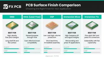
Silkscreen legends are printed via inkjet after surface finish cures.
Electrical testing (E-test) per IPC-9252B verifies opens, shorts, and netlist continuity on every bare board. SFX PCB performs 100% electrical testing (continuity and isolation) on every bare board before shipment. No defective board leaves the facility.
Boards then receive dimensional inspection and are profiled (routed or V-scored) into their final shape before packaging.
Key Factors That Affect Multilayer PCB Quality and Cost
Layer Count and Via Complexity
Each additional layer increases material cost, lamination time, and registration tolerance demands. Blind and buried vias add lamination cycles — each adding roughly a week to lead time — and require laser drilling. These are the primary cost drivers in any multilayer build.
Material Selection
Standard FR-4 isn't always sufficient. High-speed designs above 1 GHz, RF applications, and thermally demanding environments require specialty laminates. Using the wrong material causes signal loss, thermal failure, or delamination — not immediately, but inevitably.
Copper Weight
Copper weight affects more than current capacity:
- Heavier copper (2 oz, 3 oz+) requires longer etch times and affects impedance calculations
- Minimum achievable trace widths increase with copper weight (3 oz copper requires 6/8 mil minimum line/space in production)
- Mixed copper weight designs across layers add process complexity and must be explicitly called out in fabrication notes
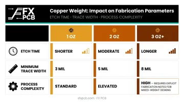
SFX PCB supports copper weights from 0.5 oz to 10 oz per layer on standard multilayer boards, with heavy copper capabilities up to 20 oz.
Impedance Control
Impedance control requires precise correlation between material dielectric constant, trace width, and layer spacing. SFX PCB offers ±10% impedance tolerance with impedance coupon testing available. Note that any material substitution mid-production invalidates the impedance calculations entirely.
Production Volume and Panel Utilization
Beyond technical specs, manufacturing economics play a significant role in total cost. Irregular board shapes and small boards without panelization waste material and drive up per-unit pricing. Early DFM consultation on panelization strategy can meaningfully reduce per-board cost at volume.
Common Misconceptions About Multilayer PCB Manufacturing
More Layers Always Means Better Performance
Each added layer increases cost, lead time, and potential failure points. The actual goal is the minimum layer count that satisfies your routing density, signal integrity, and power distribution requirements — nothing more.
Over-layering a straightforward design increases lamination risk without delivering any functional benefit.
DFM Review Is Optional — or Can Wait Until After Production Starts
Design errors that take minutes to fix at the layout stage become expensive rework orders once lamination is complete. Common examples include:
- A via landing directly on a pad
- Traces narrower than process minimums
- Unbalanced copper pours causing board warpage
DFM review is the single highest-ROI quality step in the process. SFX PCB offers free DFM analysis on every order specifically to catch these issues before a panel is touched.
Any PCB Manufacturer Can Handle Any Layer Count
Boards at 8+ layers operate under fundamentally different tolerances for registration, drilling, and plating. A manufacturer qualified for standard 4-layer work may lack the equipment or process controls to reliably produce a 16-layer impedance-controlled design.
Before committing, verify that your manufacturer holds relevant certifications — ISO 9001, ISO 13485 for medical applications, and IPC-6012 compliance — and has documented process capability at your target layer count.
Frequently Asked Questions
How is a multilayer PCB manufactured?
Multilayer PCBs are manufactured by separately imaging and etching each inner copper layer, then stacking and laminating the layers with prepreg insulating material under heat and pressure. This is followed by drilling, copper plating of via walls, outer layer processing, surface finishing, and 100% electrical testing before the boards are profiled into their final shape.
How many layers can a multilayer PCB have?
Commercial multilayer PCBs typically range from 4 to 14 layers for standard production, though specialized aerospace, server, and AI applications push well beyond that — OKI demonstrated 124-layer technology in 2025. SFX PCB supports up to 68 layers; each additional layer increases manufacturing complexity, cost, and lead time accordingly.
What materials are used in multilayer PCB manufacturing?
FR-4 fiberglass-epoxy laminate is standard for most commercial applications. Prepreg sheets bond the layers during lamination; copper foil forms the conductive traces. Rogers RO4003C and RT/duroid 5880 are selected for RF and high-frequency designs; high-Tg laminates (Tg150–180°C) are used for thermally demanding or reliability-critical applications.
What is the difference between through-hole, blind, and buried vias?
Through-hole vias pass entirely through all layers. Blind vias connect an outer layer to one or more inner layers without penetrating the full board. Buried vias connect only inner layers and are invisible from either board surface. Blind and buried vias require additional lamination cycles and laser drilling, increasing manufacturing cost and lead time.
How long does it take to manufacture a multilayer PCB?
A standard 6-layer PCB typically takes 5–10 business days, with expedited options available. Higher layer counts, blind/buried vias, and specialty materials add time — each HDI lamination cycle adds roughly one week. SFX PCB provides quotes within 24 hours of design file submission.
What is DFM analysis and why does it matter?
DFM (Design for Manufacturability) analysis is a pre-production review where the manufacturer checks design files for issues that would cause fabrication problems — undersized vias, insufficient clearances, stack-up imbalances. Catching these before production begins prevents costly rework, panel scraps, and project delays. SFX PCB provides this analysis free with every order.