This article is written for engineers, product designers, and procurement leads in medical, aerospace, automotive, and consumer electronics who are evaluating whether rigid-flex is right for their application — and want to understand what the fabrication process actually involves before committing to a design.
Key Takeaways
- Rigid-flex PCBs combine flexible polyimide layers with rigid FR4 sections into a single board, enabling 3D circuit routing without external connectors or cables
- Fabrication requires specialized processes — coverlay lamination, controlled drilling across dissimilar materials, and precision layer bonding — not found in standard PCB manufacturing
- Critical quality factors include stack-up material selection, bend radius compliance, layer registration, and via placement near transition zones
- Rigid-flex adds cost and complexity; it's the right choice only when connector elimination, tight space constraints, or harsh-environment reliability are genuine engineering requirements
- A certified manufacturer with free DFM review and 100% electrical testing on every board significantly lowers fabrication risk
What Is Rigid-Flex PCB Fabrication?
Rigid-flex PCB fabrication is the process of manufacturing boards that combine multiple layers of flexible substrates bonded to one or more rigid sections — producing a unified circuit structure rather than separate boards connected by cables.
The result is a single hybrid board that can be folded, bent, or shaped during assembly or installation while maintaining electrical continuity across both rigid and flexible regions. This construction is classified under IPC-6013E Type 4 — multilayer rigid and flexible material combinations with three or more conductive layers and plated through-holes.
How It Differs from Flex and Rigid PCBs
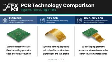
| Board Type | Construction | Best For |
|---|---|---|
| Rigid PCB | Flat FR4 laminate, no flex | Standard electronics with sufficient space |
| Flex PCB | All-polyimide, no rigid sections | Dynamic bending, continuous flex applications |
| Rigid-Flex PCB | Rigid and flex layers bonded together | 3D packaging, space-constrained assemblies, harsh environments |
Flex PCBs (IPC-6013E Types 1–3) are entirely flexible and suited to dynamic bending applications. Rigid PCBs depend on separate interconnects between boards. Rigid-flex eliminates both constraints: it accepts the added fabrication complexity in exchange for measurable gains in size reduction, weight savings, and connection reliability that neither alternative can achieve on its own.
Why Demanding Industries Choose Rigid-Flex PCBs
The industries that specify rigid-flex most consistently share a common problem: standard rigid boards with connectors cannot meet their space, reliability, or form factor requirements.
Medical devices require boards that fit inside compact, often sterile housings with no room for wire harnesses. Rigid-flex PCBs are used in defibrillators, ultrasound equipment, hearing aids, and CT scanners — applications where dimensional constraints are non-negotiable.
Aerospace and defense systems demand circuits that survive vibration, thermal cycling, and shock without connector failures. Radar systems, night vision equipment, and guided aircraft systems all rely on rigid-flex for exactly this reason.
A 2022 NASA/JPL modeling study used rigid-flex PCB structures as the basis for analyzing dynamic environment performance, confirming their suitability for the harshest operational conditions.
Consumer electronics push for thinner, lighter, foldable form factors. Sony's camera stabilizer module main board features a rigid-flex structure, enabling the compactness that modern imaging systems demand.
What Rigid-Flex Uniquely Addresses
- Eliminates wire harnesses and inter-board connectors, removing potential failure points
- Reduces solder joint count, improving signal integrity across the assembly
- Enables 3D circuit routing, distributing components across surfaces impossible with flat boards
- Reduces assembly error rates by replacing manual harness installation with a single integrated board
These advantages explain why rigid-flex is specified at the design stage in critical applications — not adopted as an afterthought when standard boards fall short.
How Rigid-Flex PCBs Are Fabricated: Step-by-Step
Rigid-flex manufacturing runs two production workflows in parallel: the flexible core (polyimide-based) and the rigid sections (FR4 or similar) are built separately, then bonded together under controlled lamination conditions. The process is longer and more sensitive to parameter variation than standard PCB fabrication.
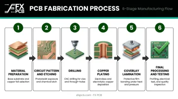
Step 1: Material Preparation
Fabrication starts with selecting and cleaning base laminate materials. Flexible layers use polyimide film with copper foil; materials like DuPont Pyralux AP (an adhesiveless all-polyimide laminate) offer copper options from 6 µm to 140 µm and dielectric thicknesses from 12 µm to 150 µm.
Rigid sections use FR4 prepreg or cores such as Isola IS410, which provides a Tg of 180°C and Td of 350°C for thermal stability.
The choice between adhesive and adhesiveless construction has downstream consequences: adhesiveless laminates offer tighter impedance control and better dimensional stability; adhesive-based constructions are more cost-effective but can affect signal performance at high frequencies.
Step 2: Circuit Pattern Generation and Etching
The copper circuit pattern is applied through photolithography, followed by chemical etching to remove unwanted copper and define traces. Both sides of the flex laminate and rigid cores are processed. Trace width and spacing tolerances in the flex region are tighter : SFX PCB holds inner layer tolerances of 3mil/3mil (1 oz) in mass production and 2.5mil/2.5mil in low-volume runs.
Step 3: Drilling
Drilling creates plated through-holes (PTHs), blind vias, and buried vias for inter-layer electrical connections. Rigid-flex boards use mechanical drilling for larger holes and laser drilling for microvias. SFX PCB supports machine drilling down to 6mil and laser drilling to 4mil for low-volume production.
The transition zones between rigid and flex regions pass through materials with different mechanical properties (polyimide vs. FR4), so drilling misalignment directly causes delamination or open circuits.
Step 4: Copper Plating
Electroless followed by electrolytic copper plating deposits copper inside drilled holes to create the PTH interconnections. Copper thickness in flex regions is intentionally thinner than in rigid sections to preserve bend performance without sacrificing conductivity.
Step 5: Coverlay Application and Lamination
Flexible regions are protected with a polyimide coverlay film rather than liquid soldermask. The coverlay is precision-cut with openings for component pads and laminated under controlled heat, pressure, and vacuum to ensure full adhesion without air pockets.
This is one of the most process-sensitive steps in rigid-flex fabrication. Rigid sections receive standard soldermask. SFX PCB's DFM review identifies coverlay opening placement issues before fabrication begins , preventing costly rework from misaligned cutouts.
Step 6: Final Processing
The final sequence includes:
- Stiffener bonding: polyimide or FR4 stiffeners applied to areas needing mechanical support
- Board profiling: CNC routing or hydraulic blanking to final board shape
- Surface finish: ENIG, immersion silver, immersion tin, or OSP on exposed pads
- 100% electrical testing: flying probe verification per IPC-9252B, confirming continuity and isolation across all nets before shipment
Key Factors That Affect Rigid-Flex Fabrication Quality
Material Stack-Up and Adhesive Selection
The stack-up choice ripples through every subsequent process step. Adhesiveless laminates like Pyralux AP provide a CTE of 25 ppm/°C below Tg and dimensional stability after etching of -0.04% to -0.08% — properties that matter in thermal cycling environments. Mismatched CTEs between rigid and flex materials are a primary cause of delamination during repeated thermal exposure.
Prepreg flow behavior during lamination affects layer bonding uniformity. Excessive resin flow into flex areas can restrict movement and compromise bend performance.
Bend Radius Compliance
Minimum bend radius for flex sections — typically around 10x the flex thickness for static bends and 20x or more for dynamic applications — must be established during design and respected throughout manufacturing. Bending at tighter radii fractures copper traces, particularly at layer transitions, making bend radius violations among the most common causes of field failures. The IPC-2223E design standard governs these requirements, but the manufacturer must also enforce them during handling and processing.
Layer Registration and Lamination Control
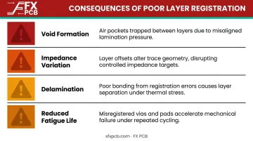
Layer-to-layer registration across rigid-to-flex transition zones directly determines bond integrity. The process requires tightly controlled temperature, pressure, and vacuum profiles. Deviations cause:
- Void formation between layers
- Impedance variation from uneven dielectric thickness
- Delamination under thermal or mechanical stress
- Reduced mechanical fatigue life
Drilling and Via Quality in Transition Zones
As I-Connect007 has reported, copper cracks and delamination can develop at the rigid-flex transition area — making via placement and drill quality near these zones a genuine risk area. Vias placed too close to the rigid-flex interface experience higher mechanical stress during bending. Annular rings in flex regions must accommodate copper foil movement without cracking.
Post-Fabrication Quality Verification
Each of these risk areas — lamination voids, via cracking, registration drift — requires active verification, not just process control. Standard inspection at a qualified manufacturer should cover:
- AOI to check trace integrity, conductor spacing, and pad geometry
- X-ray inspection to verify internal via alignment and hidden layer quality
- 100% electrical testing via flying probe, confirming continuity and isolation on every board
SFX PCB holds ISO13485 certification and performs all three as standard practice across rigid-flex orders.
What to Look for in a Rigid-Flex PCB Manufacturer
Certifications and Standards Compliance
For regulated industries, the minimum certification set to look for:
- ISO9001 — quality management system
- ISO13485 — medical device QMS (required for medical applications)
- IPC-A-610 Class 2/3 — assembly acceptance criteria
- RoHS/REACH compliance — required for global market access
These certifications reflect systematic process controls, not just final inspection. SFX PCB holds ISO9001, ISO13485, ISO14001, IPC-A-610 Class 2/3, RoHS, REACH, and UL certifications.
Fabrication Capability Range
When evaluating a manufacturer's specifications, check:
| Parameter | SFX PCB Capability |
|---|---|
| Layer count (mass production) | 2–16 layers total |
| Layer count (low volume) | Up to 20 layers total |
| Flex layers (mass production) | Up to 10 layers |
| Min trace/space (inner, mass prod.) | 3mil/3mil (1 oz) |
| Min laser drill (low volume) | 4mil |
| Max panel size | 485mm × 1500mm |
| Impedance control | ±10% |
| Surface finishes | ENIG, Immersion Silver, Immersion Tin, OSP, ENEPIG |
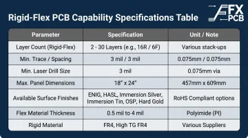
These specs matter because tighter minimums and higher layer counts let complex designs go straight to fabrication without simplification tradeoffs.
DFM Support and Prototype-to-Production Continuity
Rigid-flex designs frequently arrive at fabrication with bend radius violations, coverlay opening misalignments, or via placement errors near flex zones. A manufacturer offering free DFM analysis catches these before production begins.
SFX PCB provides free DFM review on every order, including stack-up recommendations — not just file validation. Stack-up recommendations and quotes come back within 8 hours of receiving your files.
Sourcing prototypes and production volumes from the same manufacturer eliminates the yield drops and requalification cycles that typically occur when switching suppliers between development and mass production.
Common Misconceptions About Rigid-Flex
Reliability isn't guaranteed. NASA/JPL's research documents that rigid-flex PCB systems have additional failure modes compared to traditional PCBs — specifically from interpanel contact, shearing, and frictional forces in dynamic environments. The reliability advantage applies when connector and cable failures are the dominant risk, not across every application.
Rigid-flex is not a flex board with stiffeners. These are fundamentally different constructions. Rigid-flex boards integrate FR4 or similar material as structural layers bonded within the stack-up — not attached externally. The fabrication process, material requirements, and design rules are distinct. Treating them as equivalent leads to incorrect specifications and fabrication failures.
When rigid-flex is not the right choice:
- The design fits comfortably on a standard rigid board with standard connectors
- The required bend is a one-time installation fold that a flex-to-install configuration addresses more cheaply
- Production volumes are very low and NRE cost outweighs the assembly savings
- The design team lacks the experience to manage the tighter design rules rigid-flex demands
Frequently Asked Questions
What is the difference between flex PCB and rigid-flex PCB?
Flex PCBs consist entirely of flexible polyimide substrate and are used where continuous or dynamic bending is required. Rigid-flex PCBs combine rigid and flexible layers in a single board — rigid sections carry components and provide structural support, while flex sections route electrical connections between them, enabling 3D packaging without external connectors.
What materials are rigid-flex PCBs made of?
Flexible layers use polyimide film as the substrate with copper foil conductors and a polyimide coverlay for insulation. Rigid sections use FR4 glass-epoxy laminate. Bonding layers join both during lamination — adhesiveless constructions offer better signal integrity and dimensional stability than adhesive-based alternatives.
How is a rigid-flex PCB made?
Fabrication moves through three main phases: circuit patterning and copper plating, coverlay lamination and stiffener bonding, then surface finishing and 100% electrical testing. Rigid and flex sections are built partially in parallel, then bonded together under controlled heat and pressure to form the final assembly.
How many layers can a rigid-flex PCB have?
Rigid-flex PCBs range from 2-layer designs to complex multilayer constructions of 20+ layers. SFX PCB supports up to 16 layers in mass production and up to 20 layers in low-volume runs, with flex layers up to 10 in mass production. More layers increase fabrication complexity, cost, and lead time.
What industries use rigid-flex PCBs?
Primary industries include medical devices, aerospace and defense, automotive, consumer electronics, and industrial automation. Each relies on the size, weight, and reliability advantages rigid-flex provides over traditional connector-based designs.
How long does rigid-flex PCB fabrication take?
Lead times are longer than standard rigid PCBs — typically 7 to 20 working days for production quantities depending on layer count, complexity, and surface finish. SFX PCB offers expedited prototype turns for urgent projects. Contact the team directly at info@sfxpcb.com for lead time estimates on your specific design.