
Introduction
Flex PCB prototyping is the fabrication of small-batch flexible printed circuit boards — typically 1 to 50 units — built from production-intent materials to validate electrical performance, mechanical behavior, and manufacturability before committing to full production runs.
Most engineers approach flex prototyping with rigid PCB instincts. They route traces parallel to bend axes, drop vias into flex zones, and specify electrodeposited copper where rolled annealed copper is required. These mistakes produce prototypes that pass flat inspection and fail catastrophically inside an enclosure.
This guide covers the flex prototyping process end-to-end — from design rules and material selection to what drives cost and turnaround time. If you're building for medical devices, wearables, automotive, or industrial automation, it's written for you.
Key Takeaways
- Flex PCBs require polyimide substrates and rolled annealed (RA) copper, which drives a completely different set of design rules and manufacturing steps than standard FR-4 boards
- Manufacturing runs from DFM review through photolithography, coverlay lamination, drilling, surface finish, and electrical testing — every step has flex-specific requirements
- Critical design rules: minimum bend radius, traces perpendicular to the bend axis, no vias in dynamic flex zones, stiffeners at all connector and component areas
- Cost is driven by layer count, material type, panel utilization, and surface finish — moving from one to two layers alone increases cost by 35–40%
- Flex prototyping makes sense when form factor, weight, and bend performance are core design constraints — if they're secondary considerations, rigid or rigid-flex may be the better starting point
What Is Flex PCB Prototyping and Why It Matters
What Gets Validated
A flex PCB prototype is a small-quantity build — not a breadboard approximation — using the intended production materials (polyimide film plus copper foil) to confirm what a simulation cannot: that the design holds up under real bending, real assembly conditions, and real electrical loading.
A successful prototype confirms four things:
- Electrical performance — impedance, continuity, isolation across all nets
- Mechanical compliance — bend radius adherence, delamination resistance under repeated flex
- Thermal behavior — heat distribution in constrained geometries
- Assembly compatibility — solderability, component placement accuracy in tight areas
Why Industries Are Pushing Toward Flex
The global flexible printed circuit board market was valued at USD 23.89 billion in 2024, projected to reach USD 50.90 billion by 2030 at a 13.7% CAGR. That growth reflects a real engineering shift.
Medical devices, consumer wearables, automotive systems, and aerospace applications increasingly demand circuits that conform to three-dimensional geometries, reduce harness weight, and fit into spaces where rigid boards cannot.
Flex circuits can save up to 75% of space and weight compared to conventional wire harnesses — but only when the prototype validates that the design actually performs under dynamic conditions.
Three Construction Types Worth Distinguishing
That performance depends heavily on which construction you choose. Before any design work begins, clarify the build type — it determines your material stack-up, bend radius rules, and fabrication process from the outset:
- Pure flex: polyimide throughout; suited for dynamic bending and cable replacement
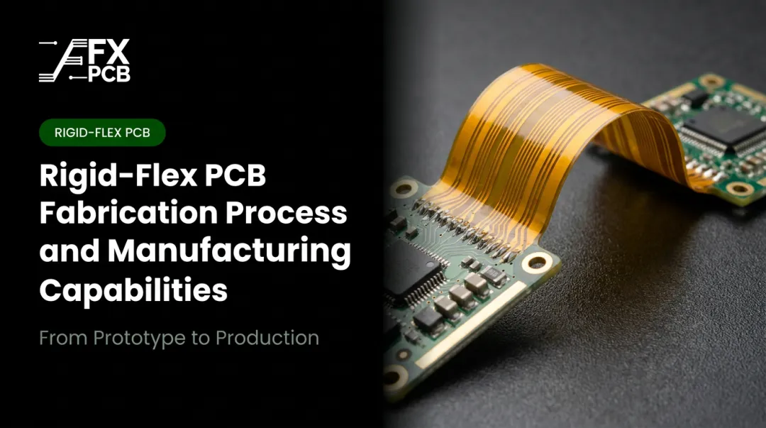
- Rigid-flex: combines FR-4 rigid sections with polyimide flex interconnects in one fabricated unit; eliminates board-to-board connectors
- Stiffened flex: adds localized FR-4 or polyimide stiffeners at connector zones without making the board fully rigid-flex
Each type carries different minimum bend radii, layer count constraints, and lamination requirements — design rules that don't transfer cleanly between them.
How the Flex PCB Prototyping Process Works
The process follows a defined sequence: DFM review → material preparation → photolithography and etching → coverlay lamination → drilling and via formation → surface finish → stiffener attachment → electrical testing and final inspection.
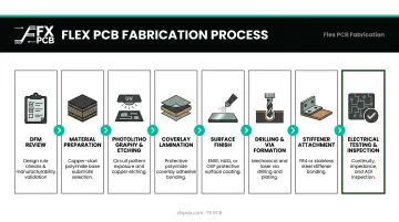
It shares some steps with rigid PCB fabrication but diverges significantly in material handling, coverlay application, and copper selection.
Step 1: DFM Review and File Preparation
Before any material is processed, the manufacturer performs a DFM review of the Gerber files, flex layer stack-up, drill data, and mechanical outline.
For flex circuits, a thorough DFM check flags:
- Vias or through-holes placed in dynamic flex zones
- Trace width and spacing violations in bend areas
- Coverlay opening misalignment with pad geometry
- Stiffener placement conflicts with the intended assembly
- Insufficient annular rings or spacing between features
SFX PCB provides a free DFM review for every order, with engineers who can identify layout issues (including trace width adjustments and stack-up configuration improvements) before tooling costs are incurred. Catching a bend zone violation at DFM costs nothing; catching it after fabrication costs time and money.
Step 2: Material Preparation and Laminate Selection
The raw materials entering a flex build are fundamentally different from rigid PCB materials:
- Substrate: Polyimide film, typically 12.5–125μm thick (DuPont Kapton HN and UBE UPILEX-S are the established reference materials)
- Conductor: Rolled annealed (RA) copper, not electrodeposited (ED) copper
RA copper's grain structure provides elongation exceeding 20%, giving it the ductility needed to survive repeated bending cycles. ED copper is more susceptible to fracturing under flex. Using it in dynamic flex zones is a common mistake that drives up rework costs.
Laminates come in adhesive-based and adhesiveless constructions. Adhesiveless laminates eliminate a layer that can degrade at high temperatures and introduce dimensional instability; they're preferred for medical and high-reliability automotive prototypes despite the cost premium.
Coverlay choice is also made here: polyimide coverlay film (mechanically cut, precisely aligned) versus liquid photoimageable solder mask. These are not interchangeable: coverlay is a structural film, not a photographic process.
Step 3: Photolithography and Etching
A photosensitive dry film is applied to the copper-clad laminate, exposed through a photomask or direct laser imaging (LDI) system, then developed. The exposed copper is etched away using alkaline chemistry, leaving the circuit pattern.
LDI is increasingly used for prototype quantities. It eliminates photomask generation costs and improves registration accuracy. KLA's LDI systems achieve line widths down to 8μm and registration accuracy of ±5μm.
SFX PCB achieves outer layer trace/space of 3mil/3mil (1oz) for prototype quantities, tightening to 2.5mil/2.5mil on inner layers for low-volume builds.
Step 4: Coverlay Lamination and Surface Finish
Coverlay, a solid polyimide film with pre-cut openings over pads, is laminated over the etched traces under heat and pressure. Unlike solder mask, which is photo-exposed, coverlay must be mechanically cut to match the pad pattern and precisely registered before lamination. Misregistration is a common yield issue in prototype runs and can render pads inaccessible.
Surface finish selection follows coverlay lamination, with the choice driven by assembly method and downstream reliability requirements:
- ENIG: Flat surface profile suits repeated soldering iterations; compatible with gold wire bonding. Per IPC-4552, specifies 3–6μm nickel beneath a minimum 0.05μm gold layer. Most commonly specified for flex prototypes.
- OSP / Immersion Silver / Immersion Tin: Cost-effective alternatives for single-reflow assemblies or short-shelf-life builds
- HASL: Generally avoided on flex due to thermal stress during the process and uneven surface profiles
SFX PCB supports all five finishes; the right choice depends on soldering iteration count, shelf life, and whether wire bonding is required.
Step 5: Drilling, Via Formation, and Stiffener Attachment
Laser drilling is preferred for flex circuits: it minimizes mechanical stress on the thin polyimide substrate and achieves smaller via diameters than mechanical drilling. SFX PCB supports laser drilling down to 4mil for prototype quantities.
After drilling, electroless copper deposition and electroplating create conductive via walls. Via placement outside dynamic flex zones is a hard rule. Plated vias in bending areas act as stress risers that initiate fracture under repeated flexing.
Stiffeners (FR-4, polyimide, or aluminum) are then laminated at connector zones and component mounting areas. FR-4 stiffeners are the most cost-effective prototype choice; polyimide stiffeners are preferred when FR-4 thickness would interfere with enclosure fit.
Step 6: Electrical Testing, AOI, and Final Inspection
Each prototype undergoes automated electrical testing to confirm open/short integrity across all nets. SFX PCB performs 100% electrical testing on every bare board, particularly important for flex prototypes where internal delamination or via fracture may not be visible on the surface.
AOI verifies trace geometry and coverlay registration. For higher-complexity builds with dense packaging, X-ray inspection provides internal layer views without damaging the board. SFX PCB performs X-ray inspection in-house, primarily for BGA verification and complex assembly review.
Essential Design Rules for Flex PCB Prototypes
Minimum Bend Radius
The bend radius is the single most critical flex-specific constraint. Violating it causes conductor cracking and delamination — often after the prototype appears functional on first inspection.
Bend radius multipliers based on layer count, per Minco and All Flex technical data:
| Construction | Minimum Bend Radius |
|---|---|
| 1–2 layer flex | 6× total stack-up thickness |
| 3+ layer flex | 12× total stack-up thickness |
| Multilayer (4+ layers) | Up to 24× total stack-up thickness |
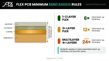
These multipliers apply to the total stack-up thickness — substrate, copper layers, coverlay, and any adhesive included. Calculate from the complete assembled dimension, not the bare polyimide film alone.
Trace Routing in Flex Zones
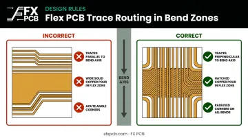
- Route traces perpendicular to the bend axis, never parallel
- Use the thinnest trace width that impedance and current requirements allow — wider traces concentrate bending stress
- Hatch or reduce copper pour in flex zones to allow uniform bending
- Eliminate acute angle corners in flex regions — these are stress concentration points that initiate cracking under fatigue
Component and Via Placement
- Keep through-hole vias, plated holes, and rigid components out of the dynamic flex zone entirely
- When a via must transition between flex and stiff zones, place it at least 1–2mm from the interface
- Mount components only in stiffened areas or on rigid sections of rigid-flex designs
Stiffener Design
Specify stiffeners for every connector attachment and component mounting zone. Misspecified stiffeners are a leading cause of prototype-to-production fit failures: include stiffener thickness, material, and placement explicitly in design files.
Stack-Up and Layer Count
Start with the simplest construction that validates the critical design intent. Engineers frequently over-specify layer count in prototypes, adding cost without improving validation value. Single-sided flex is the right starting point for most first-iteration builds. Flex prototype runs typically span 1–8 layers, with specialized multilayer builds reaching 30 layers or more when the design demands it.
Key Factors That Affect Prototype Quality and Cost
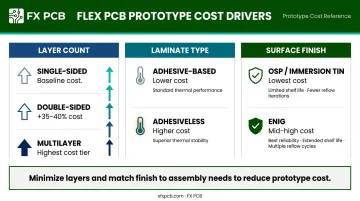
Layer count drives cost more than almost any other variable. Moving from single to double-sided flex increases cost by 35–40% per Sierra Circuits data, and each additional lamination cycle adds registration risk and delamination probability. Keeping prototype layer count to the minimum needed is both a cost and quality decision.
Panel utilization directly affects per-unit cost. Irregular board outlines, large keep-out zones, or non-standard dimensions waste panel area. Working through panelization strategy during DFM review reduces prototype unit cost. SFX PCB's maximum flex panel size is 410mm × 270mm.
Material and surface finish set the cost floor:
- Adhesiveless polyimide laminates cost more than adhesive-based but improve thermal stability
- ENIG costs more than immersion tin or OSP but delivers better reliability across multiple soldering iterations
- Aluminum stiffeners are significantly more expensive than FR-4 — for prototypes validating electrical and mechanical performance rather than production-exact spec, FR-4 stiffeners reduce cost without invalidating core test results
For turnaround time, standard single or double-sided flex designs using commonly stocked polyimide thicknesses run 3–7 business days at capable manufacturers. Multilayer flex, controlled impedance requirements, and specialty laminates extend that window.
SFX PCB's fast-turnaround flex prototyping includes board assembly from 24 hours once components are available — relevant for teams running tight iteration cycles.
Common Mistakes and When Flex May Not Be the Right Choice
Design Mistakes That Cause Prototype Failures
- Routing traces parallel to the bend axis instead of perpendicular
- Placing vias in flex zones — these crack under fatigue regardless of how clean the initial electrical test appears
- Specifying ED copper for dynamic applications instead of RA copper
- Using 90-degree corners in flex region routing
- Failing to account for bend radius in the as-assembled state — many designs pass flat inspection, then fail when first bent inside the enclosure
Process Misconceptions
- Coverlay is not solder mask. It's a solid film requiring mechanical cutting and precise registration — it cannot be photo-exposed like solder mask and won't conform to tight geometries the same way.
- Flex circuits have a finite fatigue life. Bend radius, copper weight, conductor geometry, and temperature all determine how many cycles a dynamic flex circuit can handle. Get the minimum bend radius right and you can achieve hundreds of thousands of cycles; get it wrong and cracking starts within dozens.
- Passing electrical test doesn't mean production-ready. For dynamic applications, mechanical fatigue testing under representative bending cycles is the only reliable confirmation of long-term reliability.
Beyond errors in execution, some projects shouldn't start with flex prototyping at all.
When Flex Prototyping May Not Be the Right First Step
- Thermal dissipation is a priority: Standard Kapton HN has thermal conductivity of only 0.20 W/mK — flex materials can't match metal-core rigid boards for heat management, so high-power designs warrant a different substrate
- Layer count exceeds 4–6: Designs at this density typically require rigid-flex, which adds meaningful cost and complexity before the electrical design is even confirmed
- A rigid prototype would do the job: If wired interconnects on a rigid board can validate the core electrical design, start there — flex prototyping makes sense when bending behavior and form factor are themselves part of what's being tested
Conclusion
Flex PCB prototyping works when engineers treat it as a distinct discipline, not a variation on rigid PCB design. Minimum bend radius, trace orientation perpendicular to the bend axis, via exclusion from flex zones, and proper stiffener placement aren't recommendations — they're structural requirements.
Three decisions consistently separate successful prototypes from costly respins:
- Run a DFM review before fabrication, not after
- Select the construction that matches the validation goal — don't over-specify layers or materials
- Understand the cost drivers so tradeoffs are made deliberately, not by default
SFX PCB's free DFM review, 100% electrical testing, and fast-turnaround flex fabrication give teams a concrete path from finalized design files to tested prototype boards.
When form factor, bend behavior, and weight are core product requirements, flex PCB prototyping isn't an added cost — it's the only path to a valid design validation.
Frequently Asked Questions
How flexible are flex PCBs?
Flex PCBs can bend to a minimum radius determined by stack-up thickness and layer count. They're highly conformable but not infinitely flexible. Exceeding the minimum bend radius, or bending against the grain of trace orientation, causes conductor fatigue and cracking over time.
How much does a flex PCB prototype cost?
Costs vary based on layer count, board size, material, surface finish, and quantity. Moving from single to double-sided flex alone adds 35–40% to cost, and multilayer or rigid-flex designs cost significantly more per unit at prototype quantities than at production volumes.
What is the minimum bend radius for a flex PCB?
Minimum bend radius is calculated as a multiple of total stack-up thickness: 6× for 1–2 layer dynamic applications, 12× for 3+ layers, and up to 24× for multilayer constructions. Critically, this must account for all layers (substrate, copper, coverlay, and adhesive), not just the base polyimide film.
What materials are used in flex PCB manufacturing?
Polyimide (PI) film (DuPont Kapton, UBE UPILEX-S) paired with rolled annealed (RA) copper foil is the standard for dynamic flex applications. Polyester (PET) works for static or low-temperature use at lower cost. High-frequency or RF applications call for PTFE or LCP substrates with lower dielectric loss.
How long does flex PCB prototyping take?
Standard single or double-sided flex prototypes take 3–7 business days at capable manufacturers. Multilayer flex or rigid-flex designs with controlled impedance or specialty laminates typically require 10–15 business days. Component assembly adds time depending on part availability — SFX PCB can begin assembly within 24 hours of components arriving.
What is the difference between a flex PCB and a rigid-flex PCB?
A pure flex PCB uses polyimide substrate throughout and suits dynamic bending, cable replacement, and conforming to curved surfaces. A rigid-flex PCB combines FR-4 rigid sections (stable platforms for component mounting and connectors) with polyimide flex interconnects that route through confined geometries, eliminating board-to-board connectors that would otherwise be required.