
Layer-to-layer registration accuracy is the single hardest process parameter to control in high-density PCB manufacturing. It separates suppliers with genuine HDI capability from those who claim it on a datasheet. Choosing wrong means your stack-up looks fine on paper and fails in the field.
This guide profiles five top high-density PCB suppliers evaluated specifically on alignment accuracy capabilities, enabling technology, quality certifications, and track record in demanding sectors — giving engineers and procurement teams a technically grounded starting point.
Key Takeaways
- HDI boards require layer-to-layer registration tolerances as tight as ±25 microns or better; misalignment causes via failures, signal loss, and board rejection
- Alignment accuracy depends on the supplier's technology stack: LDI systems, X-ray registration, and controlled lamination
- Top suppliers pair precision equipment with certifications (ISO9001, ISO13485, IPC-A-610) and full inspection protocols (AOI, X-ray, electrical test)
- Evaluate suppliers on documented registration tolerances, layer count capability, certifications, and industry experience
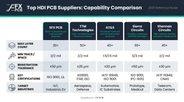
- SFX PCB, TTM Technologies, AT&S, Sierra Circuits, and Shennan Circuits are the top performers profiled here
What Makes Layer-to-Layer Alignment Critical in High-Density PCB Manufacturing
The Registration Challenge
Layer-to-layer registration is the precision with which each internal copper layer aligns with adjacent layers during lamination, measured in microns. On a 4-layer board, there's one lamination cycle and limited cumulative error.
On a 20+ layer HDI board with sequential lamination, each cycle introduces new registration variables that compound on top of previous ones.
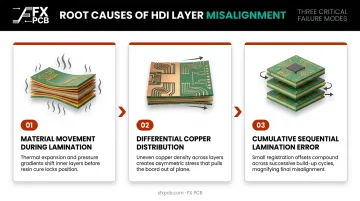
Three root causes drive misalignment in HDI structures:
- Material movement during lamination — ultra-thin cores (25–50 µm) expand and contract non-uniformly under heat and pressure
- Differential copper distribution — uneven copper density across a layer creates uneven thermal expansion, pulling registration off-center
- Cumulative sequential lamination error — each additional build-up cycle multiplies the error from previous cycles
Why It Matters for Your Design
Those root causes translate directly into design failures — and the worst ones stay invisible until electrical test or field deployment. Common consequences:
- Broken blind/buried vias — drill hits the edge of a pad instead of its center, creating an open circuit
- Impedance deviation — a misaligned reference plane shifts the effective dielectric geometry, detuning controlled-impedance traces
- Signal integrity degradation — off-center microvias create return path discontinuities, causing reflections and insertion loss in high-frequency applications like 5G mmWave and ADAS radar
Inner-layer AOI can reduce inner-layer scrap by up to 90%, according to Gardien, but only when applied before layers are committed to lamination. Catching alignment problems after lamination means scrapping the panel.
Top High-Density PCB Suppliers with Superior Layer-to-Layer Alignment Accuracy
These five suppliers were selected based on documented precision manufacturing capabilities, alignment-enabling technology, industry certifications, inspection rigor, and proven performance in demanding sectors.
SFX PCB
SFX PCB (operating as FX PCB Co.) is a Shenzhen-based full-service PCB and PCBA manufacturer with over 15 years of experience serving global electronics brands across medical devices, automotive, aerospace, telecommunications, and industrial automation. A US office in Plano, Texas provides direct support for North American engineering teams.
For alignment-critical applications, SFX PCB combines high-precision LDI systems, AOI, and X-ray inspection on every board. A free DFM analysis service proactively flags stack-up and registration risk before production begins, cutting costly re-spins at the source. All bare boards receive 100% electrical testing for continuity and isolation.
| Capability Area | SFX PCB Specifications |
|---|---|
| Layer Count | Up to 30 layers (low volume); up to 24 layers mass production; 68 layers for rigid FR4 |
| Min Trace/Space | 3/3 mil (0.075/0.075 mm) for 8-layer; ~2.76/2.76 mil for 6-layer |
| Microvia (Laser Drill) | 4 mil (0.10 mm) minimum |
| Via Structures | Blind, buried, microvias supported |
| Alignment & QC | LDI, AOI, X-ray inspection, 100% electrical test, free DFM analysis |
| Certifications | ISO9001, ISO14001, ISO13485, IPC-A-610 Class 2/3, RoHS, REACH, UL |
| Industries | Medical, Automotive, Aerospace, Telecom, Industrial Automation |
TTM Technologies
For teams sourcing at high volume with strict defense or data center requirements, TTM Technologies stands apart. One of the largest PCB manufacturers in the US, TTM has deep expertise in advanced HDI, substrate-like boards, and ultra-high layer count designs. Their end-market mix reflects where alignment precision matters most: 44% Aerospace and Defense, 24% Data Center Computing, 14% Medical/Industrial.
TTM regularly manufactures boards with more than 30 layers and can produce complex designs exceeding 70 layers. Their HDI capabilities include laser-drilled microvias down to 100 µm, any-layer via technology, and stacked copper-filled microvia structures for high-density BGA fanout.
| Capability Area | TTM Technologies |
|---|---|
| Layer Count | 30+ layers standard; 70+ layers documented |
| Min Trace/Space | 25 µm line/space (HyperBGA); 28 µm (CoreEZ) |
| Microvia | 100 µm laser-drilled; 200 µm pad diameter |
| Build-up Types | Sequential lamination, stacked microvias, any-layer via |
| Alignment & QC | Optical alignment, AOI, X-ray, electrical test |
| Certifications | ISO9001, AS9100, Nadcap, IATF, ISO13485, IPC 1791, ITAR |
| Industries | Aerospace/Defense, Data Center, Medical, Automotive |
AT&S
AT&S is an Austria-headquartered PCB manufacturer with global facilities, recognized for high-end HDI, semiconductor packaging substrates, and embedded component technologies. Their focus on ADAS, medical implants, and industrial automation requires alignment tolerances that leave no margin for field failure.
AT&S's modified semi-additive process (mSAP) achieves conductor track widths of 12 to 50 µm, and their HDI Anylayer technology uses laser-drilled microvias to connect individual layers in fully sequential build-up structures.
| Capability Area | AT&S |
|---|---|
| Min Trace/Space | 12–50 µm (SLP/mSAP); standard HDI finer than conventional |
| Build-up Types | HDI Anylayer, sequential build-up, mSAP, embedded trace substrates |
| Specialty | Embedded components, semiconductor packaging substrates |
| Alignment & QC | Sequential lamination process control, optical inspection |
| Certifications | ISO9001:2015, IATF 16949, EN 9100 (aerospace), ISO13485 |
| Industries | Automotive ADAS, Medical Implants, Industrial Automation |
Sierra Circuits
Sierra Circuits is a California-based PCB specialist focused on high-precision, high-mix manufacturing — widely recognized in the US engineering community for HDI prototyping, quick-turn production, and rigid-flex formats. Their in-house engineering team provides DFM feedback before production, a critical step for catching registration-risk stack-ups.
Sierra's LDI systems achieve approximately 5 µm variation depending on board flatness — one of the tightest documented figures from any fabricator's published data. Their HDI capability supports up to 30 layers with up to 4 lamination cycles.
| Capability Area | Sierra Circuits |
|---|---|
| Layer Count | Up to 30 layers |
| Min Trace/Space | 1.5 mil trace/space |
| Laser Drill | 3 mil (smallest); 4 mil blind-via |
| Build-up Types | 0-N-0, 1-N-1, 2-N-2; up to 4 lamination cycles |
| LDI Registration | ~5 µm variation (documented) |
| Certifications | ISO9001:2015, AS9100D, ISO13485:2016, MIL-PRF-31032, ITAR |
| Industries | Aerospace, Defense, Medical, Automotive, Consumer Electronics |
Shennan Circuits
Rounding out the list at the high-volume end, Shennan Circuits (SCC) is mainland China's leading PCB manufacturer and a global top-tier player in communication backplanes, server motherboards, and core network equipment. Their production scale supports sustained investment in alignment systems — delivering consistent registration accuracy across thousands of panels per run.
SCC publishes their registration tolerances directly: ±25 µm same-core registration and ±5 mil layer-to-layer for mass production. Layer count capability spans 2 to 68 layers in mass production and up to 120 layers for samples.
| Capability Area | Shennan Circuits |
|---|---|
| Layer Count | 2–68 layers (mass production); up to 120 layers (samples) |
| Min Laser Drill | 0.1 mm (4 mil) mass production; 0.05 mm (2 mil) samples |
| Registration Tolerance | ±25 µm same-core; ±5 mil layer-to-layer |
| HDI Capability | 4-level HDI blind hole combined structures |
| Certifications | ISO9001, IATF16949, AS9100, Nadcap, ISO13485, QC080000 |
| Industries | Telecom, Data Centers, Aerospace, Automotive, Medical |
Key Technologies That Enable Superior Layer-to-Layer Alignment
Laser Direct Imaging (LDI)
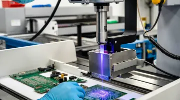
LDI is the technology benchmark to ask about first. Traditional film-mask photolithography introduces registration errors from mask warp, humidity-driven film expansion, and manual handling. LDI eliminates the mask entirely: a UV laser controlled by digital Gerber data exposes patterns directly onto the substrate.
The precision gains are significant. KLA's Orbotech Nuvogo Fine achieves ±7.5 µm registration accuracy for high-precision microvia stacking. Limata's X1000 system delivers <±25 µm outer-layer to solder-layer and <±10 µm top-to-bottom registration. LDI systems also compensate for material shrinkage and expansion in real time, scaling the image to match actual substrate dimensions after lamination — not the nominal CAD dimensions.
Optical and X-Ray Alignment Systems
LDI handles pre-lamination imaging with high accuracy, but lamination itself is a separate thermal and mechanical process that can shift inner layers relative to outer ones. Two systems address these post-lamination variables:
- CCD optical registration — Schmoll's Optiflex II punch achieves ±3 µm alignment accuracy using up to eight CCD cameras, verifying layer positioning before pressing
- X-ray post-lamination inspection — Pluritec's X-ray optimizer targets inner layers with thicknesses of 25 µm or less, compensating for both linear and non-linear deformation that optical systems can't detect
X-ray inspection is particularly critical for blind/buried via structures. Misalignment in these structures is invisible from the board surface — it only manifests as a via failure during electrical test or in the field.
Supporting Process Controls
The full alignment quality chain also requires:
- Pin-less lamination — eliminates mechanical registration pin tolerance errors that four-slot pin lamination systems can introduce
- Symmetrical stack-up construction — balances thermal expansion forces during pressing
- Pre-lamination AOI — catches pattern deviations after imaging before layers are committed to the press
Ask every supplier candidate to demonstrate each of these controls during qualification, not just claim them in a capabilities brochure.
How We Chose These Suppliers
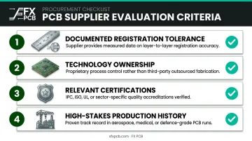
We evaluated suppliers on four criteria:
- Documented registration tolerance — ≤±25 µm demonstrated capability, with process data to back it up
- Technology ownership — in-house LDI systems, optical and X-ray registration, automated lay-up (not outsourced)
- Relevant certifications — ISO9001, ISO13485, IPC-A-610 Class 2/3, and AS9100 where applicable to target sectors
- High-stakes production history — demonstrated volume work in medical, aerospace, or automotive, where misregistration directly affects safety or function
Knowing what qualifies a supplier also clarifies what to watch out for. Three mistakes this list is designed to help you avoid:
- Selecting on price without requesting documented registration tolerance data
- Skipping DFM review before finalizing stack-up — where most alignment risks are caught cheapest
- Accepting an HDI capability claim without confirming the supplier actually owns LDI and X-ray inspection equipment and runs them at volume
Each of these gaps tends to surface as a re-spin or field failure — long after the order is placed.
Conclusion
For high-density PCB designs where layer-to-layer alignment is a functional requirement, the supplier's manufacturing technology and quality controls matter far more than name recognition or price. The five suppliers profiled here — SFX PCB, TTM Technologies, AT&S, Sierra Circuits, and Shennan Circuits — represent a verified shortlist, each with documented alignment tolerances, process capabilities, and certifications relevant to demanding applications.
Structure your supplier qualification around concrete questions: request documented registration tolerances and process capability data, confirm LDI is used for imaging, and verify X-ray inspection availability for internal layer verification. Validate certifications against your industry's requirements before committing to volume production.
Of the suppliers evaluated against those criteria, SFX PCB checks every box: over 15 years of precision HDI manufacturing, IPC-A-610 Class 2/3 compliance, free DFM analysis on every order, and 100% electrical testing on all bare boards. For teams that can't absorb alignment-related failures, that combination carries real weight from prototype through mass production. Reach out at info@sfxpcb.com or visit sfxpcb.com to request a quote.
Frequently Asked Questions
What is considered acceptable layer-to-layer alignment tolerance in high-density PCBs?
For standard multilayer boards, ±25 µm is a widely referenced benchmark — both Shennan Circuits and Limata's LDI datasheets cite this figure. For advanced HDI with stacked microvias or fine-pitch components, tolerances tighten to ±7.5 µm or better. Always ask suppliers to provide process capability data (Cpk reports) rather than accepting a quoted specification at face value.
How does LDI improve alignment accuracy compared to traditional film-based methods?
LDI eliminates film masks entirely, removing distortion errors from humidity, temperature, and manual handling, and exposes patterns directly from digital Gerber data with real-time substrate shrinkage compensation. Sierra Circuits documents approximately 5 µm LDI variation; KLA's Nuvogo Fine achieves ±7.5 µm, both well below the ±25 µm or worse typical of film-based photolithography.
What certifications indicate rigorous quality controls for high-density PCB manufacturing?
ISO9001 covers general quality management; ISO13485 applies specifically to medical device manufacturing; IPC-A-610 Class 2/3 governs assembly workmanship standards; AS9100D addresses aerospace and defense requirements. Verify that certifications are current and scoped specifically to PCB fabrication or assembly — not just the broader parent company.
How does layer misalignment affect signal integrity in high-frequency PCB applications?
Misaligned layers cause impedance deviation by shifting the effective dielectric geometry, while off-center microvia landing pads create return path discontinuities that generate signal reflections and insertion loss. In high-frequency applications such as 5G mmWave, high-speed SerDes, and ADAS radar, these effects degrade bit error rates and link margins at the system level.
What is the difference between HDI PCBs and standard multilayer PCBs?
HDI boards use laser-drilled microvias (≤150 µm diameter per IPC-2226A), blind and buried via structures, sequential lamination, and fine trace/space geometries at or below 3 mil/3 mil. Standard multilayer boards rely on mechanically drilled through-hole vias, conventional imaging, and wider geometries, making them less suited to high-density BGA fanout and miniaturized designs.
How can I verify a PCB supplier's layer registration accuracy before placing a volume order?
Request Cpk process capability reports and cross-section microsection samples showing layer-to-layer alignment, then review X-ray inspection reports on sample boards. Start with a prototype run with registration tolerance requirements explicitly documented in your purchase specification — this establishes a measurable acceptance baseline before committing to volume.