
Most buyers discover the gap between "quoted lead time" and "actual delivery date" only after it's already caused a schedule slip. A manufacturer quoting "24-hour" fabrication isn't promising boards on your doorstep tomorrow. That clock often starts after engineering review, assumes complete files, and doesn't include assembly or shipping.
IPC's July 2024 supply chain survey found 52% of electronics manufacturers reporting rising material costs and 32% seeing supplier inventory declining—conditions that directly affect whether your quoted lead time holds.
This article breaks down what actually drives PCB lead times, what realistic timelines look like from US-serving manufacturers, and how to structure your orders to avoid the most common delay triggers.
Key Takeaways
- Quick-turn bare board fabrication for 2–4 layer designs runs 24–48 hours at fast-turn US manufacturers—once files clear review and are approved
- Prototype PCB assembly adds 48–72 hours once all components and complete files are confirmed in hand
- Design complexity, material selection, file completeness, and component availability drive the most variation in your timeline
- "Quick-turn" buys queue priority, not faster manufacturing steps—the process itself doesn't compress
- Submitting DFM-ready files and designing to standard materials consistently beats paying for expedited services after the fact
What Is a PCB Lead Time and Why Does It Matter?
PCB lead time is best understood as the time from a clean, manufacturable release package to shipment—not from the moment you upload files. Most manufacturers start the fabrication clock only after Gerber files are received, reviewed, and approved by engineering—a detail that's easy to overlook when comparing quoted turnarounds.
Two Lead Time Categories That Get Confused
| Type | Volume | Queue | Primary Use |
|---|---|---|---|
| Prototype | Small batches | Faster | Design iteration and validation |
| Production | High volume | Longer | Launch-ready manufacturing |
Mixing up these two categories when planning a product launch is one of the most common scheduling mistakes hardware teams make.
Why Lead Times Are Less Predictable Than They Used to Be
Supply chain conditions since 2020 have made "standard" lead times harder to pin down. IPC data shows persistent pressure on material costs and inventory levels across both APAC and North American supply chains.
A board that shipped in two weeks previously might now carry a four-week lead time due to laminate availability or component sourcing delays. None of that shows up in a manufacturer's published quick-turn pricing.
Before locking a production timeline, always confirm:
- Material availability for your specific laminate and stackup
- Component stock status, especially for long-lead or allocated parts
- Whether the quoted lead time covers fabrication only or includes assembly
Typical PCB Lead Times from US Manufacturers
Lead times vary significantly by board type, service tier, and manufacturer. The table below reflects ranges from published manufacturer data—treat these as starting points for planning, not guarantees.
| Board Type / Stage | Quick-Turn | Standard |
|---|---|---|
| 2–4 layer bare board | 24–48 hours | 3–5 days |
| 6–8 layer bare board | 72 hours (urgent) | 7 days |
| 10+ layer / HDI | 96 hours (urgent) | 10–15 days |
| Prototype PCBA (2–4 layers) | 48 hours* | 5–12 days |
| Prototype PCBA (6–8 layers) | 72 hours* | 7–12 days |
| High-volume production | Quote-dependent | Weeks to months |
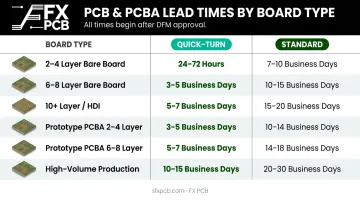
*Once all components are in hand and files have passed DFM review. Source: Sierra Assembly, PCBWay Quick Turn
What "Quick-Turn" Actually Means
Not all manufacturers define quick-turn the same way. Some apply it only to bare board fabrication. Others include assembly. Before accepting a fast lead time quote, confirm:
- Does it include both fabrication and assembly, or just one?
- When does the clock start—at order placement or after engineering approval?
- What happens if DFM review flags an issue?
The Shipping Gap
Manufacturer lead time quotes don't include shipping. For overseas manufacturers shipping to the US via express carriers (DHL, FedEx, UPS), add 3–7 business days. Domestic US manufacturers have shorter transit times, but don't assume same-day handoff to a carrier.
That distinction matters when evaluating overseas options too. SFX PCB, for example, fabricates in Shenzhen and ships direct to US customers via DHL, FedEx, and UPS — with order management and engineering support handled through its Plano, TX office. Transit time adds to the total; fabrication speed depends on factory capacity and process complexity either way.
What Happens at Each Stage of the PCB Lead Time
Total lead time is sequential. A hold at any stage pushes every stage after it. Understanding where delays actually occur helps you protect the schedule.
Pre-Production: DFM Review, File Validation, and Material Readiness
This is the most overlooked delay source, and it happens before the fabrication clock even starts.
Pre-production includes:
- Gerber file review and validation
- BOM completeness check (manufacturer part numbers, approved alternates)
- Pick-and-place file verification against assembly drawing
- Design for Manufacturability (DFM) analysis for spacing, annular rings, trace widths, and stackup
A DFM issue caught after production begins can add 24 hours to several days depending on the severity and how quickly the design team responds. SFX PCB performs free DFM analysis on every order, with engineering feedback typically returned within 24 hours of file submission—which means issues get surfaced before they hit the production queue rather than inside it.
Fabrication
Fabrication runs sequentially through these core steps:
- Inner layer imaging and etching
- Lamination and drilling
- Plating, solder mask, and surface finish
- Silkscreen and electrical testing
Each additional layer, via type, or specialty process adds cumulative time. A standard 2-layer FR4 board clears this process in hours. A 12-layer HDI board with controlled impedance and blind/buried vias is a different story—Sierra Circuits notes that HDI boards with stacked or staggered microvias require sequential lamination with anywhere from 2 to more than 4 cycles depending on design complexity.
SFX PCB performs 100% electrical testing on every bare board before it moves to assembly or ships.
Assembly, Testing, and Shipping
Once bare boards clear electrical testing and all components are physically on hand, assembly begins.
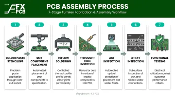
The assembly sequence:
- Solder paste stenciling
- SMT component placement
- Reflow soldering
- Through-hole insertion (if applicable)
- AOI inspection
- X-ray inspection (for BGAs and complex assemblies)
- Functional testing (per customer specification)
AOI runs as standard after soldering. X-ray is used for complex multilayer boards and BGA components. Functional testing (FCT) is available on request and runs to your specifications, simulating real operating conditions.
Shipping is a discrete phase—build it into your timeline as a separate line item.
Key Factors That Affect Your PCB Lead Time
Board Complexity
Layer count and via architecture have the most direct impact on fabrication time:
- 2–4 layer standard boards: 24–48 hours quick-turn
- 6–8 layer boards: 72 hours urgent, 7 days standard
- 10+ layer / HDI with blind/buried vias: 96+ hours urgent, 10–15 days standard
Controlled impedance adds a stackup approval step before fabrication begins. Finalize impedance requirements before layout release, not after.
Material Selection
Standard FR4 with common copper weights moves fastest because it's in stock. Specialty substrates—Rogers, ceramic, Taconic, PTFE—require procurement and extend lead times regardless of what quick-turn pricing says.
SFX PCB supports FR4 (Kingboard, Nanya, Shengyi), Rogers, ceramic, and PTFE substrates for US customers. Standard FR4 projects typically aren't affected by stock delays. For specialty materials, confirm procurement lead time before committing to a schedule.
File Completeness
Every back-and-forth between buyer and manufacturer pauses the clock. Common file issues that trigger holds:
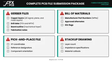
- Gerbers missing layer definitions or drill data
- BOM line items without manufacturer part numbers or approved alternates
- Pick-and-place files with coordinate errors or missing reference designators
- Undefined component substitutes for EOL or hard-to-source parts
Submit Gerber or ODB++, drill files, stackup drawing, complete BOM with MPNs, and pick-and-place files together. Don't make the manufacturer ask for them.
Component Availability
In turnkey assembly, every BOM line item must be available before production starts. One long-lead component can hold the entire order, even if the bare boards are already fabricated.
SFX PCB's sourcing team has access to over 600,000 stocked components, which reduces fulfillment time on most standard parts. For uncommon or allocated components, run an AVL and lifecycle check before placing the assembly order.
Order Timing and Queue Position
Most manufacturers have daily cut-off times for quick-turn orders. Submit after the cut-off and you're queued for the next business day. At high-volume periods, even quick-turn orders may wait in queue.
Watch for these timing variables that often go unnoticed:
- Daily cut-off windows: Most quick-turn fabs have hard cut-offs between 2–5 PM local time
- Holiday and peak periods: Q4 and pre-summer volume spikes can push even urgent orders back 1–2 days
- Revision cycles: A single DRC correction or BOM update resets your queue position
Common Misconceptions About US PCB Lead Times
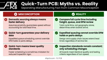
"Domestic automatically means faster." US manufacturers eliminate ocean freight time — typically 5–10 days saved on transpacific routes. But fabrication involves the same process steps regardless of where the factory is located. A US manufacturer advertising 5-day fabrication isn't faster than an overseas manufacturer with 3-day fabrication—it's slower on that metric, even accounting for express shipping from overseas.
The honest comparison is: domestic fab time + domestic shipping versus overseas fab time + 3–7 business days express shipping. Run the numbers for your specific order before assuming domestic is faster.
"Paying for quick-turn guarantees a delivery date." Expedited service buys queue priority, not process acceleration. If your files trigger a DFM hold or a component is unavailable, the premium you paid doesn't help. Teams that submit clean, complete files on standard turns often receive boards faster than teams that paid for quick-turn but had design errors.
"Quick-turn means lower quality." This concern is understandable, but reputable manufacturers don't relax inspection standards under time pressure. Quick-turn and standard orders go through the same process: IPC-A-610 review, AOI, and electrical testing. What changes is scheduling priority, not rigor. SFX PCB holds IPC-A-610 Class 2/3 compliance across all orders regardless of turn time.
To summarize where these misconceptions break down:
- Speed: Domestic eliminates freight time, not fabrication time — compare total cycle, not one leg
- Quick-turn guarantees: Expedited queuing can't override DFM holds or parts delays
- Quality: Inspection standards don't scale with lead time — schedule does
How to Plan Smarter and Reduce Your PCB Lead Time
The highest-leverage lead time reduction strategy costs nothing: eliminate delay triggers before you submit the order.
Before submitting any order:
- Confirm Gerber package includes all copper layers, drill files, board outline, and fabrication notes
- Verify BOM includes manufacturer part numbers and at least one approved alternate for every component
- Validate pick-and-place file against the assembly drawing
- Request a DFM check—before committing to a production timeline, not after
Specify FR4 with standard copper weights and HASL or ENIG surface finish unless your application requires otherwise. Check the manufacturer's material availability before finalizing your stackup. A Rogers laminate that needs to be procured can add 1–2 weeks before fabrication even begins.
Material choices happen at the design stage, but supplier relationships pay dividends at every stage after. Teams that pre-qualify a manufacturing partner—verified capabilities, established file handoff workflows, validated quality standards—experience shorter effective lead times because engineering review is faster and communication friction is lower.
SFX PCB supports that kind of relationship with 24-hour assembly capability (once parts are in hand), free DFM review on every order, and a US office in Plano, TX for same-time-zone support on quick-turn decisions. For hardware teams iterating fast without switching manufacturers between prototype and production, that continuity matters.
Frequently Asked Questions
What are typical lead times for US PCB manufacturers?
Quick-turn bare board fabrication for 2–4 layer designs runs 24–48 hours at fast-turn services; 6–8 layer boards take 72 hours urgent or 7 days standard. Prototype PCBA adds 48–72 hours once parts are in hand. These are fabrication timelines—shipping is additional.
Can I get a PCB made in 24 hours in the USA?
Yes, for simple 2–4 layer rigid boards with standard FR4, complete Gerber files, and no DFM issues. Full assembly in 24 hours also requires all components to be in stock and files to clear engineering review without revision.
What is the difference between PCB fabrication lead time and assembly lead time?
Fabrication covers bare board production; assembly is the separate process of populating the board with components. Total project lead time adds fabrication, assembly, and shipping together. That distinction matters because manufacturers often quote only one phase in their headline number.
How does board complexity affect PCB lead time?
Each additional layer, specialty via type (blind, buried, microvia), controlled impedance requirement, or specialty material adds process steps and queue time. Simple 2-layer boards complete in hours; HDI designs with multiple lamination cycles may take 5–10 days or more.
Does the choice of surface finish affect lead time?
HASL finishes process faster than ENIG or hard gold, which require additional chemistry steps. Specialty finishes may also be subject to facility-specific material availability. Confirm finish availability when you confirm your stackup.
What happens if my design fails the DFM check?
The manufacturer halts production pending design clarification or correction. Depending on the severity and response time, this adds 24 hours to several days. Submit your Gerbers for DFM review before locking in your schedule — most issues surface within hours and are far cheaper to fix at that stage.