This guide covers the properties that actually matter for RF material selection, how those properties behave in real operating conditions (not just on datasheets), the major laminate families and where they fit, and the manufacturing realities that separate a board that works in simulation from one that works in the field.
Key Takeaways
- Select RF substrates based on Dk, Df, CTE, Tg, thermal conductivity, and copper profile rather than cost alone
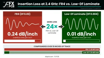
- Target Dk below 4 and Df below 0.005 for RF/microwave applications; FR4's Df of ~0.02 causes 24× more insertion loss than a Df 0.004 material at 2.4 GHz
- PTFE materials (Rogers RT/duroid, RO3000 series) deliver the best electrical performance for demanding RF applications
- RO4000-series hydrocarbon-ceramic laminates balance RF performance with standard FR4 processability
- Dk and Df shift with frequency, temperature, moisture, and aging — build those tolerances into your design margins
- Engage your fabricator before finalizing the stackup — RF laminates require specialized processes that not every facility supports
What RF PCB Materials Are and Why Standard FR4 Falls Short
RF PCB materials are substrate laminates engineered to maintain controlled, stable dielectric behavior from roughly 500 MHz up through the mmWave range. Standard FR4 is an epoxy-glass composite — it was designed for structural integrity, moisture resistance, and flammability rating, not for signal transmission at frequency.
The electrical gap is measurable and consequential. According to Microwave Journal, standard FR4 has an epsilon-r of approximately 4.6 and a loss tangent of 0.04, with practical use generally limited below 3 GHz because insertion loss increases rapidly above that threshold.
Three loss mechanisms explain why FR4 degrades at RF frequencies:
- Dielectric loss — molecular dipoles in the epoxy matrix absorb energy as they realign with the oscillating field; absorption increases with frequency
- Conductor loss — the skin effect concentrates current at the trace surface, and FR4's rough copper foil amplifies this loss; the rougher the copper, the worse the effect
- Radiation loss — at GHz frequencies, traces begin acting as unintentional antennas, radiating energy rather than transmitting it
Those three mechanisms combine into a hard number: insertion loss. Rogers modeling data shows that at 2.4 GHz on a 50-ohm line, a material with Df 0.02 (typical FR4 territory) produces 0.24 dB/inch of insertion loss — compared to just 0.01 dB/inch for a Df 0.004 material. That's not a marginal difference. At 5G infrastructure frequencies, automotive radar bands (76–81 GHz), or any mmWave application, that gap compounds across every inch of trace — which is why material selection is the first engineering decision, not an afterthought.
Key Electrical and Physical Properties Governing RF Material Performance
RF material performance is defined by the interaction of electrical and thermal-mechanical properties. Optimizing one without the others produces boards that perform in simulation and fail in deployment.
Dielectric Constant (Dk) and Its Real-World Variability
Dk is the ratio of material permittivity to free-space permittivity. It controls:
- Signal propagation velocity (higher Dk = slower signals)
- Characteristic impedance (higher Dk = narrower traces for the same impedance)
- Capacitive coupling between adjacent conductors
Target Dk below 4 for RF work. FR4's Dk varies from roughly 4.7 at low frequencies to below 4.4 at high frequencies — a variability exceeding ±5% — while high-performance RF materials typically hold Dk tolerance below ±2%.
Four factors cause Dk to deviate from the nominal datasheet value:
- Material anisotropy — woven glass reinforcement creates direction-dependent Dk; the value perpendicular to the fiber weave differs from the value parallel to it
- Temperature — FR4 Dk can shift by up to 400 ppm/°C; RO3003 and RO4350B change by roughly 40 ppm/°C and 50 ppm/°C respectively, making them far more stable
- Frequency (dispersion) — Dk decreases as frequency increases; values measured at 1 MHz are not valid at 10 GHz
- Moisture absorption and aging — absorbed water raises the effective Dk; thermal cycling causes slow resin changes over time
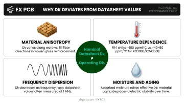
Design margins must account for all four. Build in tolerance stack analysis using worst-case Dk values across your operating temperature range and frequency band — not just the nominal datasheet figure.
Dissipation Factor (Df) and Insertion Loss
Df (loss tangent) measures how much energy the dielectric absorbs per signal cycle. At RF frequencies, rapidly oscillating fields force molecular dipole realignment in the resin, converting signal energy directly to heat. Higher Df means higher attenuation and more heat generation within the substrate.
Target Df below 0.005 for RF and microwave work. For power amplifier applications below 6 GHz, Rogers specifies Df ≤ 0.005 as adequate.
Df and copper profile jointly determine insertion loss — this is where many designs go wrong. When you select a very low-Df PTFE laminate, conductor loss from rough copper foil becomes the dominant loss mechanism.
Rogers copper foil data illustrates this starkly: at 90 GHz, a 50-ohm line on 4 mil LCP measures 2.2 dB/inch with rolled copper versus 3.7 dB/inch with standard ED foil. High-profile copper can also raise the apparent effective Dk by nearly 10%. Low-profile copper grades — VLP, HVLP, or reverse-treated foil (RTF) — are essential companions to low-Df laminates, particularly above 10 GHz.
Thermal-Mechanical Properties: CTE, Tg, and Thermal Conductivity
Three thermal-mechanical properties determine whether an RF board survives real-world operating conditions — not just whether it passes initial electrical tests.
| Property | Target Value | What Happens If Missed | Notable Examples |
|---|---|---|---|
| CTE (X/Y axis) | Close to copper (~17 ppm/°C) | Via and microvia pad stress during reflow | RT/duroid 5880: 237 ppm/°C Z-axis — needs careful via design |
| CTE (Z-axis) | Below 70 ppm/°C | Cracked vias under thermal cycling | PTFE laminates often exceed this; design margins required |
| Tg | Above 170°C | Delamination, Z-axis expansion, via cracks above transition temp | RO4350B: >280°C; I-Tera MT40: 200°C |
| Thermal conductivity | Above 0.5 W/mK | Heat buildup in high-power PA applications | RO4003C: 0.71 W/mK; I-Tera MT40: 0.61 W/mK (most materials: 0.2–0.3 W/mK) |
CTE mismatch is particularly dangerous in hybrid stack-ups that combine PTFE-based RF layers with standard FR4 core materials. The Z-axis expansion differential accelerates via fatigue across thermal cycles — a failure mode that rarely appears during bench testing but surfaces in field deployments.
Major RF PCB Material Families: Characteristics and Use Cases
No single RF laminate wins across all dimensions. The right choice is always application-specific, frequency-specific, and dependent on your fabricator's process capabilities.
PTFE-Based Materials
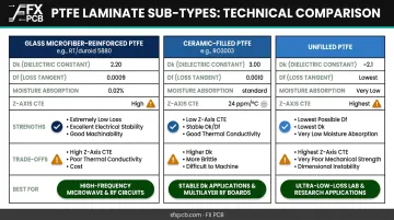
PTFE (polytetrafluoroethylene) is the reference material for high-frequency design. Its chemical inertness means minimal molecular interaction with EM fields, which translates directly to low Df. Three PTFE sub-types address different needs:
| Sub-type | Characteristics | Trade-offs |
|---|---|---|
| Glass microfiber-reinforced PTFE (e.g., RT/duroid 5880) | Dk 2.20, Df 0.0009 at 10 GHz; 0.02% moisture absorption | Z-axis CTE 237 ppm/°C; more demanding to fabricate |
| Ceramic-filled PTFE (e.g., RO3003) | Dk 3.00, Df 0.0010 at 10 GHz; Z-axis CTE only 24 ppm/°C | Slight Df penalty vs. unfilled; drill wear from ceramic filler |
| Unfilled PTFE | Lowest Dk (~2.1), lowest Df | Highest CTE; most difficult to process; limited dimensional stability |
All PTFE variants share one fabrication requirement: drilled holes must be chemically or plasma pre-treated before electroless copper deposition. Sodium naphthalene treatment must not exceed 30 seconds; plasma treatment uses approximately 4,000 W at 40 kHz for 10–30 minutes. Skipping this step results in failed copper adhesion.
RT/duroid 5880 is the go-to for aerospace, defense, and precision test equipment. RO3003's improved CTE behavior makes it more practical for complex multilayer builds.
Rogers RO4000 Series and Hydrocarbon-Ceramic Laminates
Where PTFE dominates on electrical performance, the RO4000 series wins on manufacturability. It occupies the commercial RF sweet spot: near-PTFE electrical performance with standard FR4 processability. It requires no plasma pre-treatment and works with standard drilling parameters — the primary reason RO4000-series materials dominate commercial RF production.
Key specs:
- RO4003C: Dk 3.38 ±0.05, Df 0.0027 at 10 GHz, thermal conductivity 0.71 W/mK, Z-axis CTE 46 ppm/°C
- RO4350B: Dk 3.48 ±0.05, Df 0.0037 at 10 GHz, Tg >280°C, moisture absorption 0.06%
RO4350B is the most widely fabricated commercial RF laminate. SFX PCB regularly processes both RO4350B and RO4003C for RF, microwave, and telecommunications applications.
Alternative Suppliers: Isola, Panasonic Megtron, and LCP
Isola I-Tera MT40 RF/MW: Dk 3.45, Df 0.0031 at 10 GHz, Tg 200°C, thermal conductivity 0.61 W/mK. A thermoset alternative that processes like FR4 while delivering competitive RF performance. A strong alternative when Rogers isn't your fabricator's default.
Panasonic Megtron 6 (R-5775): Dk 3.4, Df 0.004 at 12 GHz, Tg 185°C, moisture absorption just 0.01%. Primarily positioned for high-speed digital, but suitable for lower-frequency RF circuits. Its very low moisture absorption is an advantage in humid environments.
LCP (liquid crystal polymer): Dk approximately 3, loss tangent below 0.004, stable from DC to 110 GHz with very low moisture absorption. An emerging substrate for millimeter-wave and flexible RF applications where conventional laminates struggle.
Rogers is not always the correct answer. Supplier selection should follow the application, the insertion loss budget, and what your fabricator can actually process reliably.
When FR4 Remains Acceptable
FR4 and enhanced variants (such as FR408HR) are appropriate in specific situations:
- Sub-1 GHz RF applications with relaxed loss budgets
- Non-RF layers in hybrid stack-ups (power planes, digital control layers)
- Cost-constrained consumer IoT where frequency and power levels permit
- Mixed-signal boards where RF traces are isolated to premium laminate layers
In hybrid stack-ups, RF-grade material covers only the layers carrying RF signals. Standard laminate handles the rest. This approach can meaningfully reduce material cost compared to building the entire board in premium laminate, though it introduces fabrication complexity that requires early coordination with your manufacturer.
Selecting the Right RF Material: A Decision Framework
Start with your insertion loss budget, not with brand preference. Work backward from the maximum allowable signal attenuation at your highest operating frequency to determine the maximum acceptable Df. Then shortlist materials that meet that constraint — and only then apply secondary filters.
Secondary filter criteria:
- Verify Tg exceeds maximum operating temperature by at least 25°C to prevent delamination under thermal stress
- Minimize Z-axis CTE mismatch between stack-up materials to protect vias during thermal cycling
- Confirm available laminate thicknesses support your target impedance at your intended trace geometry
- For outdoor, airborne, or marine hardware, treat moisture absorption as a primary criterion — RO3003 showed roughly 0.1 dB/inch additional loss at 79 GHz after 72 hours at 85°C/85% RH
The over-specification trap: Choosing the highest-performance material available for every application is not good engineering. RT/duroid 5880 is unnecessary for a 2.4 GHz WiFi module. Over-specified materials add cost, create potential yield issues at fabricators unfamiliar with their processing requirements, and may introduce compatibility problems in hybrid builds. Match material to frequency range, power level, volume, and production environment.
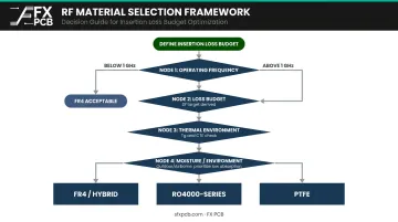
That material-matching discipline becomes most critical in hybrid stack-ups, where RF-grade laminate covers RF signal layers and standard material handles power and ground. Engage your fabricator before finalizing the stack-up design — different materials laminate at different pressures and expand at different rates, requiring adjustments to scaling and drill parameters.
Running a DFM analysis at this stage pays off directly. SFX PCB offers free DFM review on every order, and catching material incompatibility before tooling is committed is far less expensive than resolving it after.
Manufacturing Realities and Common Misconceptions
Fabrication Challenges Specific to RF Materials
- PTFE pre-treatment: All PTFE drilled holes require chemical or plasma treatment before metallization — skipping this step causes copper adhesion failure, making it a hard process requirement.
- Ceramic-filled laminate drilling: Ceramic fillers in RO3003 and similar materials cause accelerated carbide drill bit wear. Rogers fabrication guidelines specify maximum hit counts of 300 for 0.060-inch stacks and only 100 for 0.180-inch stacks — significantly lower than FR4 limits.
- Impedance control: SFX PCB's standard impedance tolerance is ±10%, verified using TDR or VNA equipment. For RF designs requiring tighter control, discuss specific requirements before order placement.
- Hybrid stack-up lamination: Combining materials with different CTEs demands precise lamination pressure profiles and scaling compensation. Plan hybrid builds collaboratively with the fabricator from the stackup stage to manage these variables before they become yield problems.
Three Misconceptions That Cause Specification Errors
Misconception 1: Datasheet Dk and Df are fixed values. Datasheet values are measured at a specific frequency (often 10 GHz for Rogers materials) and a specific temperature — not yours. Always verify values at your actual operating frequency and temperature range. FR4 Dk shifts from ~4.7 at low frequencies to below 4.4 at high frequencies, a variation that changes trace impedance in ways simulation tools won't catch if fed the wrong input.
Misconception 2: Lower-Df material automatically means lower insertion loss. Not if the copper profile doesn't match the laminate. At low Df values, conductor loss from rough standard copper foil dominates total insertion loss. A Signal Integrity Journal case study on Isola I-Tera MT40 found that mixing smoother signal copper with rougher reference planes produced higher-than-expected insertion loss — the low-Df laminate's benefit was partially negated by copper profile inconsistency in the build.
Misconception 3: Lab impedance results transfer directly to field conditions. Temperature shifts Dk. Moisture uptake raises it. Long-term resin aging changes it further.
A board that hits impedance targets in a controlled lab may drift outside spec after six months of field exposure. Design margins must account for all three effects — particularly for mmWave applications, where a 5% Dk shift translates directly to a measurable impedance deviation.
Validation Methods for Fabricated RF Boards
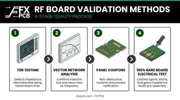
Addressing these misconceptions at the design stage only goes so far — validation after fabrication confirms the board actually performs as specified. Key methods include:
- TDR (Time-Domain Reflectometry): Identifies impedance discontinuities along transmission lines; effective for detecting process-induced deviations
- Vector network analysis: Measures S-parameters (insertion loss, return loss) to confirm the fabricated board meets frequency-domain specifications
- Production panel coupons: Dedicated test structures fabricated alongside production panels allow non-destructive material and process verification without consuming production boards
- 100% bare board electrical testing: Catches opens, shorts, and gross impedance deviations before assembly — essential for RF boards where a single defective trace can compromise the entire RF path
Conclusion
RF PCB material selection is a governing design decision. The substrate's Dk, Df, CTE, Tg, copper profile, and moisture behavior collectively determine whether the fabricated board meets its performance targets under real conditions, not just at room temperature during initial test.
Treat datasheet values as starting points with known sources of variation, not as guarantees. Before committing to layout, build margins for each failure mode and verify that your fabricator can actually execute the process:
- Account for frequency dispersion and thermal drift across the operating range
- Factor in moisture absorption effects, especially for outdoor or high-humidity deployments
- Confirm fabrication process spread with your specific manufacturer's tolerances
- Validate that the facility has the process controls to fabricate your chosen material correctly
The right material on paper is the wrong choice if the manufacturing facility can't hold the tolerances it requires.
Frequently Asked Questions
What are RF PCBs?
RF PCBs are specialized circuit boards designed to transmit and receive high-frequency signals — typically 500 MHz and above — used in applications like mobile communications, radar, and GPS. Unlike standard digital boards, they require controlled dielectric materials, precise impedance management, and tightly toleranced fabrication processes.
What is the best material for RF PCBs?
There is no single best material. Rogers RO4350B is the most widely used commercial RF laminate due to its balance of electrical performance and standard processability. RT/duroid 5880 suits aerospace and defense applications requiring very low loss. The correct choice depends on operating frequency, insertion loss budget, thermal environment, and production volume.
What is the difference between Dk and Df in RF PCB materials?
Dk (dielectric constant) controls signal propagation speed and trace impedance — lower Dk means faster signals and wider traces for a given impedance target. Df (dissipation factor) controls how much signal energy the material absorbs and converts to heat. Both should be minimized for RF work, with practical targets of Dk below 4 and Df below 0.005.
Can FR4 be used for RF PCB applications?
FR4 is acceptable for sub-1 GHz RF applications and for non-RF layers in hybrid stack-ups. Above that threshold, its Dk of ~4.6 and Df of ~0.04 cause significant attenuation and dispersion. For 5G, automotive radar, mmWave, or any precision RF circuit, dedicated RF-grade laminates are required.
What is a hybrid RF PCB stack-up and when should I use it?
A hybrid stack-up combines RF-grade laminates on signal layers with standard FR4 on power, ground, and digital control layers. It suits mixed-signal designs where only specific layers need RF-grade dielectric performance, cutting material cost without compromising electrical performance where it counts.
How does copper surface roughness affect RF PCB performance?
At high frequencies, the skin effect confines current to the conductor surface, making copper roughness a direct source of loss. Rogers data shows that at 90 GHz, standard ED copper produces 3.7 dB/inch of insertion loss versus 2.2 dB/inch for rolled copper on the same substrate. Above 10 GHz, conductor loss can exceed dielectric loss, making low-profile copper grades (VLP, HVLP, RTF) as important a choice as the laminate itself.