HDI PCB Fabrication
Manufacture dense multilayer boards with fine line/space capability, laser drilling, controlled stackups, and advanced surface finishes for compact electronics requiring reliable interconnect performance.

Build dense, signal-critical electronics with high density PCB services engineered for advanced impedance control, reliable fabrication, and scalable production. FX PCB supports complex multilayer designs, fine line/space requirements, laser drilling, high-frequency materials, and rigorous electrical testing to help engineering teams reduce rework, protect signal integrity, and move from prototype to market-ready boards with confidence.
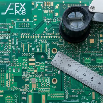
Precision PCB fabrication solutions for dense layouts, signal integrity, manufacturability, and production-ready reliability.
Manufacture dense multilayer boards with fine line/space capability, laser drilling, controlled stackups, and advanced surface finishes for compact electronics requiring reliable interconnect performance.
Support high-speed signal paths with carefully engineered trace geometry, dielectric selection, layer stack design, and verification practices that help maintain stable impedance across critical nets.
Produce high-frequency and complex multilayer PCBs for telecommunications, industrial automation, automotive, medical, and advanced electronics applications where signal stability and low loss matter.
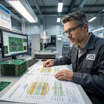
We review Gerber files, stackup requirements, drill data, impedance targets, and manufacturing constraints. Free DFM analysis helps identify spacing, via, material, or trace-width risks before production begins.
FX PCB combines engineering discipline, certified quality systems, and direct manufacturing strength.
Over 15 years of PCB and PCBA manufacturing experience for demanding global industries.
ISO9001, ISO14001, ISO13485, UL, RoHS, and REACH support regulated product requirements.
Free DFM analysis helps reduce redesigns, rework, and signal-integrity manufacturing risks.
Move from prototype to mass production through one direct manufacturing partner.
Engineering-focused support for precision electronics manufacturing.
FX PCB has built its reputation over more than 15 years in PCB and PCBA manufacturing, evolving from a PCB fabricator into a comprehensive electronics manufacturing partner. With dedicated PCB and PCBA factories in Shenzhen, China, and a US office in Plano, Texas, the company supports global engineering teams across consumer electronics, automotive, medical devices, industrial automation, telecommunications, aerospace, and defense. Its vision is to bridge the gap between innovative concepts and market-ready products through reliable fabrication, rigorous quality systems, responsive support, and scalable production capabilities that help customers launch with fewer delays and greater confidence.
Impedance control in PCB manufacturing means designing and fabricating traces so high-speed signals encounter a predictable electrical resistance along the transmission path. It depends on trace width, copper thickness, dielectric material, layer spacing, and stackup structure. For dense or high-frequency boards, controlled impedance helps reduce reflections, signal loss, timing errors, and communication failures.
Send your design files for expert engineering review.

Quality management for consistent PCB manufacturing.

Environmental responsibility across manufacturing operations.

Recognized safety compliance for electronic products.
Share your Gerber files, stackup requirements, impedance targets, and production goals. FX PCB will review your project and provide practical guidance for manufacturable, reliable boards.
For immediate assistance, feel free to give us a direct call at (+1) 5103455000. You can also send us a quick email at info@sfxpcb.com.
For immediate assistance, feel free to give us a direct call at (+1) 5103455000. You can also send us a quick email at info@sfxpcb.com.