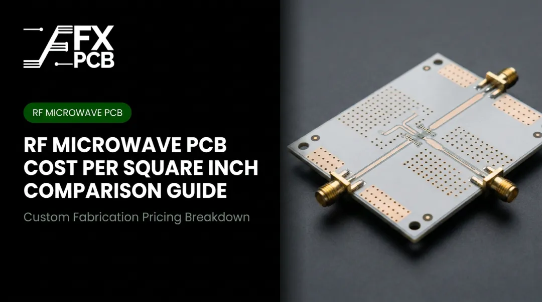

These boards require specialty laminates, tighter dimensional tolerances, and multi-step validation testing that standard PCB production simply doesn't involve. The result: lead times that regularly surprise engineers who are used to FR4 turnarounds.
This guide breaks down realistic lead time ranges for RF and microwave PCBs, the specific factors that extend timelines beyond standard production, and concrete strategies to cut turnaround without touching signal integrity.
Key Takeaways
- RF/microwave PCB lead times typically run 5–14 days for prototypes; complex multilayer hybrid stackups can reach 15–25+ days
- Specialty laminate procurement (Rogers, Taconic) is the top delay driver; non-stocked materials add 5–10 working days before fabrication starts
- Controlled impedance requirements add process steps and mandatory TDR verification that standard PCBs don't require
- Incomplete design files cause the most preventable delays—incomplete impedance callouts can hold an order in pre-production indefinitely
- A manufacturer with in-house RF laminate stock and direct engineering access removes the two biggest lead time variables
Why RF Microwave PCBs Take Longer Than Standard PCBs
The root cause is physics, not just complexity.
Standard FR4 PCBs operate at frequencies where material properties are relatively forgiving. At GHz frequencies, every material parameter matters. Rogers specifies RO4350B at Dk 3.48 ±0.05 and Df 0.0037 at 10 GHz—tight values that require precise process control to maintain through fabrication. Deviation from those specs can render a design non-functional, not just degraded.
Material Sourcing: The First Delay
FR4 laminates are commodity materials stocked globally. RF-grade laminates are not. Rogers RO4350B, RO4003C, Taconic, and Arlon substrates are specialty items. Manufacturers who don't stock them must order from distributors—and non-stocked materials like TMM, AD, CLTE, or CuClad families can add 5–10 working days through authorized distributor procurement.
That delay happens before a single drill bit touches your board.
Impedance Control Adds Process Steps
RF PCBs require controlled impedance—typically 50Ω to ±5% or tighter per IPC-2141. Hitting that tolerance requires:
- Pre-production stackup modeling and trace width calculation
- Precision etching process control during fabrication
- Post-fabrication TDR (Time Domain Reflectometry) verification on impedance test coupons
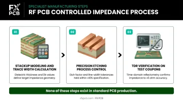
None of these steps exist in standard PCB production, and none can be skipped.
DFM Issues Hit RF Designs Harder
RF PCB designs surface manufacturability problems more often during engineering review. Common issues include:
- Impedance mismatches from under-specified callouts
- Insufficient ground plane coverage
- Trace geometries that can't hold tolerance at available copper weights
- Via stub effects that weren't modeled during design
According to Sierra Circuits, unclear impedance callouts can hold an order in pre-production until the stackup and BOM are resolved. Each revision cycle typically costs 1–3 business days.
High-Reliability Applications Add Documentation Requirements
Aerospace, defense, and medical RF boards don't just need fabrication. They need:
- ISO 13485 QMS compliance for medical device supply chains
- AS9100D quality management for aviation, space, and defense
- MIL-PRF-31032D qualification inspection for military printed boards, including lot conformance and first article inspection
- Environmental testing: thermal cycling, moisture resistance, dielectric withstanding voltage
Standard commercial PCBs require none of this. For high-reliability RF applications, these requirements are fixed costs that extend timelines regardless of how efficient the fabrication process is.
RF Microwave PCB Lead Time Benchmarks
Lead times vary significantly by board complexity. Here's a practical reference framework based on published manufacturer data:
| Board Type | Typical Lead Time | Notes |
|---|---|---|
| 2-layer RF prototype (simple microstrip, test fixture) | 3–7 working days | Faster when Rogers/Taconic materials are in stock |
| 4–6 layer RF with controlled impedance | 7–12 working days | TDR verification and ENIG finish add processing time |
| Complex multilayer hybrid (PTFE + FR4, 8+ layers) | 15–25+ working days | Sequential lamination cycles, plasma desmear for PTFE holes |
| Aerospace/medical with FAI and environmental testing | Add 5–10 working days to above | Documentation, first article inspection, qualification testing |
A few important clarifications on these ranges:
Prototype runs (1–10 boards) can often be expedited. Production runs require panel optimization, yield planning, and scheduling—which adds time but reduces per-unit cost.
PTFE also carries a specific processing requirement. Rogers' fabrication guidelines for CLTE-series PTFE laminates require sodium or plasma pretreatment of drilled holes before conductive seed-layer deposition—a step that adds roughly 1–2 working days for plasma desmear.
ENIG is the preferred surface finish for RF boards—its flatness and consistent conductivity matter at high frequencies. MCL notes ENIG is a more complex finishing process than HASL, and Microwave Journal guidance emphasizes that finish selection should account for application requirements, material supplier input, and fabricator recommendations. Factor in an extra 1–2 days compared to HASL when scheduling.
Lead time starts when clean files are approved—not when the order is placed. Epec's manufacturing guidance describes a "day zero vs. day one" distinction: the clock starts when a complete, approvable data package is received, the PO is accepted, and open questions are resolved.
Submitting incomplete Gerber files, missing impedance specifications, or an unresolved stackup can add 2–5 days before production even begins.
Key Factors That Drive RF Microwave PCB Lead Times
Specialty Material Procurement
PTFE-based and ceramic-filled laminates from Rogers, Taconic, Arlon, and Isola aren't commodity items. For manufacturers without standing inventory, distributor procurement alone can consume most of a week.
There's also an important distinction within the RF laminate category:
- Rogers RO4350B uses standard epoxy/glass processing and doesn't require specialized through-hole treatments. It's faster to process than pure PTFE.
- PTFE-based materials (RO3000 series, RT/duroid, CLTE) are mechanically softer, require sodium or plasma hole pretreatment, and may need more stringent rinse and bake cycles for ceramic-filled variants.
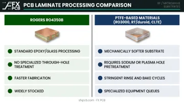
Manufacturers without dedicated RF processing lines may need to schedule PTFE boards into specialized equipment queues, extending throughput time beyond the material procurement delay.
Layer Count and Stackup Complexity
Hybrid stackups combining PTFE RF layers with FR4 control layers require sequential lamination—multiple press cycles where each adds curing, cooling, inspection, and re-registration time before the next layer set can proceed. Sierra Circuits documents support for up to four sequential lamination cycles for RF/microwave builds.
Each press cycle is a time multiplier, not just an additive delay. A 12-layer hybrid board with three lamination cycles doesn't take three times as long as a 4-layer board—but it takes substantially longer than most engineers anticipate during planning.
That extended fabrication timeline feeds directly into what happens next: a longer post-fabrication testing chain.
Impedance Testing and Quality Validation
The post-fabrication testing chain for RF PCBs typically includes:
- 100% electrical continuity testing on bare boards
- TDR impedance verification on fabricated test coupons
- Insertion loss and return loss measurement where specified
- Environmental stress testing (thermal cycling, humidity resistance) for aerospace/medical
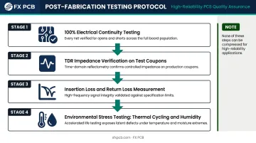
This testing chain adds days to the final delivery schedule. For high-reliability applications, none of these steps can be compressed—TDR verification exists precisely because impedance deviations don't show up until the board is in a live RF circuit.
DFM Review and Design Iteration
RF PCB designs surface DFM issues at higher rates than standard digital designs. The most common findings during engineering review include:
- Trace geometries that can't hold impedance tolerance at the specified copper weight
- Insufficient separation between RF and digital ground planes
- Via stub effects that degrade high-frequency signal integrity
- Reference plane discontinuities near connector footprints
The cost isn't just the correction itself. It's the review restart. Each iteration cycle—issue identified, design corrected, review begins again—typically costs 1–3 business days. Two or three cycles across a project adds up to a week or more of preventable delay.
How to Reduce Your RF Microwave PCB Lead Time
Submit a Complete File Package
Incomplete files are the most common preventable cause of lead time delays. Before submitting an order, verify your package includes:
- Gerber RS-274X or X2 files (or ODB++ / IPC-2581)
- Drill files
- IPC-356 netlist
- Full stackup specification with material callouts
- Impedance targets (value, trace width, layer, tolerance)
- Surface finish specification
- Any special fabrication notes (via fill, controlled depth, etc.)
Sierra Circuits' controlled impedance documentation guidance is direct: unclear impedance callouts hold orders in pre-production because the stackup and BOM can't be confirmed. "Controlled impedance to 50Ω" without specifying which traces, which layers, or reference planes isn't an actionable specification. It's a delay trigger.
Use DFM Analysis Before Production
Mid-production revision cycles typically add 1–3 days per round-trip — and most stem from issues a DFM review would have caught upfront. SFX PCB provides free DFM analysis with every order, covering trace geometry, stackup configuration, and design specifications before fabrication begins. Catching a stackup mismatch at review costs hours; catching it during production costs days and restarts.
Choose Materials Manufacturers Stock
Specifying commonly stocked materials, where RF performance allows, eliminates procurement lead time entirely. Within the Rogers RO4000 series, RO4350B and RO4003C are the most widely stocked grades. Choosing these over lower-volume specialty materials avoids distributor procurement delays without compromising performance for most applications.
SFX PCB manufactures Rogers RO4000 series boards and actively works with both RO4350B and RO4003C variants. For material availability on your specific project, their team replies within 12 hours of file submission.
Separate Prototype and Production Strategies
For prototypes, accept that expedited turnaround carries a cost premium. Use that phase to validate your design fully before committing to production volumes. For production runs, communicate volume forecasts to the manufacturer early so materials can be pre-staged and production slots reserved.
Discovering a stackup issue mid-production run is not a 1–3 day revision cycle. It triggers a full requalification event.
Standardize RF Design Rules Across Projects
Repeating design patterns across projects lets manufacturers reuse engineering setup work instead of starting from scratch each time. On derivative or follow-on designs, this reduces review time by a day or more. Specific elements worth standardizing:
- Trace widths and copper weights
- Impedance targets (50Ω for most RF signal lines)
- Stackup configurations and material selections
- Via types and tolerances
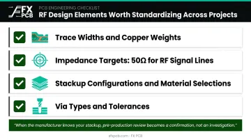
When the manufacturer already knows your stackup and requirements, pre-production review becomes a confirmation, not an investigation.
What to Look for in an RF Microwave PCB Manufacturer
Quoted lead time and real lead time diverge when a manufacturer lacks the right capabilities. Evaluate these specifically:
RF laminate inventory: Does the manufacturer stock Rogers and Taconic materials in-house, or must they order from distributors? In-house stock can cut days from your schedule before fabrication even begins.
Dedicated impedance control processes: Can they hold ±5% impedance tolerance? Do they perform TDR verification in-house, or outsource it? In-house TDR capability means faster results and direct communication when issues arise.
Direct engineering access: Can you speak with an engineer when design questions come up, or does everything route through a quoting portal? SFX PCB provides direct engineering support for each customer, so design questions get answered quickly rather than queued behind a ticketing system.
Relevant certifications: Match certifications to your application:
- ISO 9001 — baseline quality management
- ISO 13485 — required for medical device supply chains
- IPC-A-610 Class 2/3 — assembly acceptance standard
- IPC-6012 — rigid board fabrication qualification
SFX PCB holds ISO 9001, ISO 13485, and IPC-A-610 Class 2/3 certifications. Manufacturers who already hold the certifications your application requires don't need additional qualification steps that would otherwise add weeks to a project.
Prototype-to-production continuity: Switching manufacturers between prototype and production resets the engineering review and qualification process. SFX PCB handles both prototype and high-volume production, so the engineering setup, material knowledge, and qualification work from your prototype phase carries directly into production. No requalification cycle, no restart.
Frequently Asked Questions
What is the lead time for PCB manufacturing?
Standard PCB lead times range from 24 hours for simple 2-layer prototypes to 3–4 weeks for complex multilayer RF boards. The final timeline depends on layer count, material type, quantity, and testing requirements. RF and microwave boards sit at the longer end due to specialty materials and mandatory validation testing.
How long does it take to manufacture an RF microwave PCB prototype?
RF microwave prototypes typically take 5–14 days depending on complexity. Simple 2-layer boards using stocked Rogers materials can often be expedited to 3–7 days, while boards requiring PTFE laminates, controlled impedance, and TDR verification generally run 10–14 days minimum.
Why do RF microwave PCBs take longer than standard PCBs?
Three factors drive longer timelines:
- Material procurement: Rogers and Taconic laminates aren't stocked like FR4, adding 5–10 days for non-stocked materials
- Tighter tolerances: Additional process steps are required to hit RF-grade dimensional specs
- Mandatory testing: Post-fabrication TDR verification and impedance testing that standard PCBs don't require
What materials cause the longest delays in RF microwave PCB production?
PTFE-based laminates — Rogers RO3000 series, RT/duroid, and Taconic materials — are the main sources of delay when not stocked on-site. Ceramic-filled substrates and hybrid stackup materials requiring sequential lamination add further procurement and processing time beyond standard RF laminates.
Can I get expedited manufacturing for RF microwave PCBs?
Yes. For simpler 2-layer configurations with stocked materials, expedited service can reduce turnaround to 3–7 days. Rush services carry a cost premium, and boards requiring aerospace or medical certification cannot have QC steps compressed without compromising reliability.
How does DFM analysis reduce RF microwave PCB lead time?
DFM analysis identifies manufacturability issues—impedance mismatches, trace geometry problems, stackup errors—before production begins, preventing revision cycles that each cost 1–3 days. Manufacturers who include DFM as a standard step consistently deliver RF boards on shorter, more predictable timelines than those who treat it as optional.